
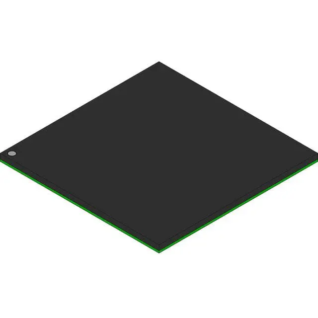
画像は参照用のみです。
EPM570F256C5N
IC CPLD 440MC 5.4NS 256FBGA
- メーカー
- Mfr。パート #EPM570F256C5N
- パッケージ BGA-256
- データシート
- 在庫中5723
100% オリジナル &新しい
出荷の準備ができている24時間
365日の保証
RFQおよびもっと割引を得る
仕様
| Package | Tray |
| Series | MAX® II |
| ProductStatus | Active |
| ProgrammableType | In System Programmable |
| DelayTimetpd(1)Max | 5.4 ns |
| VoltageSupply-Internal | 2.5V, 3.3V |
| NumberofLogicElements/Blocks | 570 |
| NumberofMacrocells | 440 |
| NumberofI/O | 160 |
| OperatingTemperature | 0°C ~ 85°C (TJ) |
| MountingType | Surface Mount |
| Package/Case | 256-BGA |
概要
Description
The EPM570F256C5N is a member of the Altera MAX 10 FPGA family, designed for low-power, high-performance applications. It features 256,000 logic elements, integrated flash memory, and flexible I/O options, making it suitable for a variety of applications, including industrial automation, automotive, and consumer electronics.
Key characteristics include its support for various I/O standards, built-in digital signal processing (DSP) capabilities, and advanced power management features. The device is available in a compact form factor and is optimized for low static and dynamic power consumption, making it suitable for battery-operated devices.
The EPM570F256C5N is programmed using standard HDL languages like VHDL or Verilog and is compatible with various development tools from Intel (formerly Altera), facilitating rapid design and prototyping. Its architecture allows for easy modification and scalability, making it a versatile choice for engineers looking to implement complex digital logic designs efficiently.
Features
The EPM570F256C5N is a MAX 10 FPGA (Field Programmable Gate Array) from Intel (formerly Altera). Key features include:
1. Logic Elements: It contains 5,760 logic elements, allowing for complex digital designs.
2. Memory: Supports up to 256 KB of embedded memory blocks, enabling efficient data storage and manipulation.
3. I/O Pins: Offers up to 80 user-configurable I/O pins, facilitating various interface options.
4. Programming: Comes with a flash-based architecture for non-volatile configuration, ensuring the design remains intact after power loss.
5. Speed Grade: Operates at a speed grade of 5, providing a balance of performance and power consumption.
6. Power Efficiency: Low power consumption, making it suitable for battery-powered and portable applications.
7. Integrated Features: Includes PLLs (Phase-Locked Loops) and clock management for enhanced performance.
8. Development Tools: Compatible with Intel Quartus Prime software for design implementation and simulation.
These features make the EPM570F256C5N suitable for a wide range of applications, including industrial, automotive, and consumer electronics.
Package
The EPM570F256C5N is packaged in a Fine-Pitch Quad Flat Package (FQFP) with a 256-pin configuration.
Pinout
The EPM570F256C5N is an FPGA (Field Programmable Gate Array) from Altera (now part of Intel). It features a pin count of 256. The device is part of the MAX 10 family, which integrates logic elements, memory blocks, and DSP blocks suitable for various applications.
The main functions of the EPM570F256C5N include:
- Implementation of custom logic circuits.
- I/O configuration for interfacing with other devices.
- Support for various communication protocols.
- Integration of embedded memory and DSP capabilities for signal processing.
This FPGA is designed for low-power applications and provides in-system reconfiguration, making it versatile for a range of designs from simple to complex. Its programmability allows users to tailor the hardware to specific needs, enhancing design flexibility.
Manufacturer
The EPM570F256C5N is manufactured by Altera Corporation, which is a subsidiary of Intel Corporation. Altera specializes in programmable logic devices, including FPGAs (Field-Programmable Gate Arrays) and CPLDs (Complex Programmable Logic Devices). The EPM570F256C5N is part of Altera’s MAX 10 family, designed for various applications such as digital signal processing, automotive, and consumer electronics. Altera focuses on providing innovative solutions for designers in the semiconductor industry, enabling them to create customizable hardware for a wide range of applications.
Application
The EPM570F256C5N is a versatile FPGA (Field-Programmable Gate Array) used in various application areas, including industrial automation, automotive systems, telecommunications, consumer electronics, and medical devices. Its flexibility allows for custom hardware design, signal processing, and real-time control in embedded systems, making it suitable for tasks like data processing, system-on-chip designs, and rapid prototyping.
Equivalent
The EPM570F256C5N is a MAX 10 FPGA from Intel (formerly Altera). Equivalent products include the Lattice iCE40 series, Xilinx Spartan-6, and Xilinx Artix-7 FPGAs, which offer similar functionalities and performance for low-to-mid range applications. Always check specific features, I/O capabilities, and power requirements for the best match for your project.
出荷
出荷方法私たち
DHL、FedEx、TNT、UPS、またはあなたの選択の他の運送業者を通じてグローバルな出荷サービスを提供します。
出荷料参照(DHL/FedEx):
DHL の: 配送費は25ドル〜45ドル(0.5kg)の範囲で、推定配送時間は2〜5営業日です。
フェデックス: 配送費は25ドル〜40ドル(0.5kg)の範囲で、推定配送時間は3〜7営業日。
UPS の: 配送費は25ドル〜45ドル(0.5kg)の範囲で、推定配送時間は3〜7営業日。
TNT社: 配送費は25ドル〜65ドル(0.5kg)の範囲で、推定配送時間は3〜7営業日。
EMS: 配送料金は30〜50ドル(0.5kg)の範囲で、推定配送時間は7〜15営業日です。
登録航空郵便: 配送費は2〜4ドル(0.1kg)で、推定配送時間は5〜20営業日です。
支払い
Payment Methods
支払い期間は100%前払いです。
現在、下記の支払い方法のみを受け入れています。:
1. ペイパル
2. クレジット・デビットカード
3. ワイヤー 転送
類似
-
![MX25V1635FZNQ03]() MX25V1635FZNQ03
Macronix
-
![MX25V5126FM1I]() MX25V5126FM1I
Macronix
-
![MX25V16066M1I02]() MX25V16066M1I02
Macronix
-
![MX25R3235FZNIL0]() MX25R3235FZNIL0
Macronix
-
![MX25R6435FBDIL0]() MX25R6435FBDIL0
Macronix
-
![MX29GL512FHXFI-11G]() MX29GL512FHXFI-11..
Macronix
-
![MX25U51279GXDR00]() MX25U51279GXDR00
Macronix
-
![MX25R1635FZUIH0]() MX25R1635FZUIH0
Macronix
-
![MX25V1635FM2I]() MX25V1635FM2I
Macronix
-
![MX25L12833FM2I-10G]() MX25L12833FM2I-10..
Macronix
-
![MX25L12833FZNI-10G]() MX25L12833FZNI-10..
Macronix
-
![MX25U25645GXDI00]() MX25U25645GXDI00
Macronix








