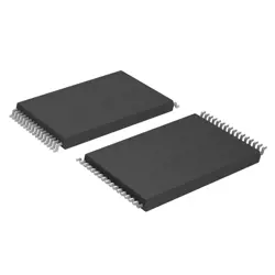
画像は参照用のみです。
EP4SGX530KH40I3N
IC FPGA 744 I/O 1517HBGA
- メーカー
- Mfr。パート #EP4SGX530KH40I3N
- パッケージ BGA-1517
- データシート
- 在庫中7978
100% オリジナル &新しい
出荷の準備ができている24時間
365日の保証
RFQおよびもっと割引を得る
仕様
| Package | Tray |
| Series | Stratix® IV GX |
| ProductStatus | Obsolete |
| NumberofLABs/CLBs | 21248 |
| NumberofLogicElements/Cells | 531200 |
| TotalRAMBits | 28033024 |
| NumberofI/O | 744 |
| Voltage-Supply | 0.87V ~ 0.93V |
| MountingType | Surface Mount |
| OperatingTemperature | -40°C ~ 100°C (TJ) |
| Package/Case | 1517-BBGA, FCBGA |
概要
Description
The EP4SGX530KH40I3N is a member of Altera’s Stratix IV FPGA family, designed for high-performance applications. It features a high-density architecture with 530,000 logic elements, offering extensive resources for complex designs. The device operates at a maximum speed of up to 40 GHz and supports advanced digital signal processing (DSP) capabilities, making it suitable for applications like telecommunications, data centers, and high-end computing.
Key features include multiple I/O standards, integrated multipliers, and memory blocks, which enhance its versatility for various applications. The FPGA is optimized for low power consumption, making it ideal for energy-efficient designs.
Its modular architecture supports extensive customization, allowing developers to tailor the functionality to specific needs. The EP4SGX530KH40I3N is particularly valuable in scenarios requiring high data throughput and processing capabilities. Overall, this FPGA provides a robust solution for developers looking to leverage programmable logic in demanding environments.
Features
The EP4SGX530KH40I3N is a field-programmable gate array (FPGA) from Altera's Stratix IV series. Key features include:
1. Logic Elements: Approximately 530,000 logic elements (LEs) for complex designs.
2. High-Speed I/O: Supports a variety of I/O standards, including LVDS, with a maximum I/O count of around 1,100 pins.
3. Memory: Integrated with up to 20 Mbits of embedded memory, ideal for high-performance applications.
4. DSP Blocks: Contains around 1,200 dedicated DSP blocks for efficient digital signal processing.
5. Front-End DSP: Supports high data rates and complex algorithms, suitable for communication and multimedia tasks.
6. Power Efficiency: Designed for lower power consumption while maintaining performance.
7. Flexible Configuration: Can be configured for various applications ranging from telecommunications to data processing.
These features make the EP4SGX530KH40I3N suitable for high-performance computing, signal processing, and custom hardware applications.
Package
The EP4SGX530KH40I3N is packaged in a FGG676 form factor, which is a fine-pitch ball grid array (FBGA) package. This type of package provides high pin density and is suitable for high-performance applications.
Pinout
The EP4SGX530KH40I3N is a Stratix IV FPGA from Intel (formerly Altera) with 530,000 logic elements. It features a total pin count of 1152.
The functions of its pins include:
- I/O Pins for interfacing with external devices.
- Power Supply Pins for VCC and ground connections.
- Configuration Pins for programming the FPGA, including JTAG and other modes.
- Clock Pins for input clock signals and global clock distribution.
- Dedicated Functional Pins for specific functions like PLLs, SERDES, and other specialized features.
These pins support a wide range of applications in digital design, including communication, signal processing, and control systems.
Manufacturer
The EP4SGX530KH40I3N is manufactured by Intel Corporation, specifically under its Altera product line. Intel is a multinational corporation headquartered in Santa Clara, California, primarily known for designing and manufacturing semiconductor products, including microprocessors, chipsets, and programmable logic devices (PLDs). The Altera line, acquired by Intel in 2015, focuses on Field Programmable Gate Arrays (FPGAs) and related technologies, which are used in various applications such as telecommunications, automotive, industrial automation, and consumer electronics. Intel operates in the technology sector, emphasizing research and development, innovation, and production of advanced integrated circuits.
Application
The EP4SGX530KH40I3N is a Stratix IV FPGA from Intel, commonly used in high-performance computing, telecommunications, video processing, and industrial automation. Its application areas include data processing, signal processing, ASIC emulation, and prototyping, as well as network infrastructure and embedded systems. The device’s high speed and flexibility make it suitable for applications requiring real-time data handling and complex algorithm implementations.
Equivalent
The EP4SGX530KH40I3N is an FPGA from Intel's Stratix IV family. Equivalent products may include:
1. Xilinx Kintex-7: Offers similar performance and features.
2. Lattice ECP5: Comparable in low-power applications.
3. Microsemi SmartFusion2: Integrates FPGA with ARM Cortex-M3.
Check specific requirements like I/O count, power consumption, and application needs for the best fit.
1. Xilinx Kintex-7: Offers similar performance and features.
2. Lattice ECP5: Comparable in low-power applications.
3. Microsemi SmartFusion2: Integrates FPGA with ARM Cortex-M3.
Check specific requirements like I/O count, power consumption, and application needs for the best fit.
出荷
出荷方法私たち
DHL、FedEx、TNT、UPS、またはあなたの選択の他の運送業者を通じてグローバルな出荷サービスを提供します。
出荷料参照(DHL/FedEx):
DHL の: 配送費は25ドル〜45ドル(0.5kg)の範囲で、推定配送時間は2〜5営業日です。
フェデックス: 配送費は25ドル〜40ドル(0.5kg)の範囲で、推定配送時間は3〜7営業日。
UPS の: 配送費は25ドル〜45ドル(0.5kg)の範囲で、推定配送時間は3〜7営業日。
TNT社: 配送費は25ドル〜65ドル(0.5kg)の範囲で、推定配送時間は3〜7営業日。
EMS: 配送料金は30〜50ドル(0.5kg)の範囲で、推定配送時間は7〜15営業日です。
登録航空郵便: 配送費は2〜4ドル(0.1kg)で、推定配送時間は5〜20営業日です。
支払い
Payment Methods
支払い期間は100%前払いです。
現在、下記の支払い方法のみを受け入れています。:
1. ペイパル
2. クレジット・デビットカード
3. ワイヤー 転送
類似
-
![MX25V5126FM1I]() MX25V5126FM1I
Macronix
-
![MX25V4035FZUI]() MX25V4035FZUI
Macronix
-
![MX25V2033FM1I]() MX25V2033FM1I
Macronix
-
![MX25V16066M2I02]() MX25V16066M2I02
Macronix
-
![MX25L25673GMI-10G]() MX25L25673GMI-10G
Macronix
-
![MX25U6435FM2I-10G]() MX25U6435FM2I-10G
Macronix
-
![MX29LV160DTTI-70G]() MX29LV160DTTI-70G
Macronix
-
![MX29F040CTI-70G]() MX29F040CTI-70G
Macronix
-
![MX25U51245GZ4I00]() MX25U51245GZ4I00
Macronix
-
![MX25R4035FM1IL0]() MX25R4035FM1IL0
Macronix
-
![MX25U3232FM2I02]() MX25U3232FM2I02
Macronix
-
![MX29LV040CQI-70G]() MX29LV040CQI-70G
Macronix