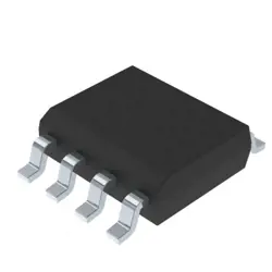
画像は参照用のみです。
EP3SL150F780I3N
IC FPGA 488 I/O 780FBGA
- メーカー
- Mfr。パート #EP3SL150F780I3N
- パッケージ 780-BBGA, FCBGA
- データシート
- 在庫中7297
100% オリジナル &新しい
出荷の準備ができている24時間
365日の保証
RFQおよびもっと割引を得る
仕様
| Supplier | Intel |
| Package | Tray |
| Series | Stratix® III L |
| ProductStatus | Obsolete |
| NumberofLABs/CLBs | 5700 |
| NumberofLogicElements/Cells | 142500 |
| TotalRAMBits | 6543360 |
| NumberofI/O | 488 |
| Voltage-Supply | 0.86V ~ 1.15V |
| MountingType | Surface Mount |
| OperatingTemperature | -40°C ~ 100°C (TJ) |
| Package/Case | 780-BBGA, FCBGA |
概要
Description
EP3SL150F780I3N is a Lattice Semiconductor FPGA in the ECP3SL family. It targets high-density, low-power digital logic in a 780-ball fine-pitch BGA package. The “150” indicates about 150k logic elements, suitable for complex logic, memory interfacing, and DSP-style blocks. The suffix I3N denotes industrial temperature grade with RoHS-compliant packaging; F780 confirms the 780-ball package.
Key features (typical): configurable logic blocks, Block RAM, DSP resources, multiple I/O banks with various I/O standards, and clocking resources (PLLs). It’s designed for applications in networking, video/graphics, data processing, and embedded systems where density matters.
Design flow: HDL (Verilog/VHDL) coding, synthesis/mapping with Lattice Diamond (or compatible tools), placement & routing, bitstream generation, and programming via JTAG or non-volatile memory.
For exact specifications, pinout, and reference designs, consult the EP3SL150F780I3N datasheet and user guide.
Key features (typical): configurable logic blocks, Block RAM, DSP resources, multiple I/O banks with various I/O standards, and clocking resources (PLLs). It’s designed for applications in networking, video/graphics, data processing, and embedded systems where density matters.
Design flow: HDL (Verilog/VHDL) coding, synthesis/mapping with Lattice Diamond (or compatible tools), placement & routing, bitstream generation, and programming via JTAG or non-volatile memory.
For exact specifications, pinout, and reference designs, consult the EP3SL150F780I3N datasheet and user guide.
Features
EP3SL150F780I3N is a Cyclone III FPGA. Key features:
- 150K logic elements
- 780-pin FineLine BGA package
- Industrial temperature range (-40°C to 85°C)
- Multiple clock management blocks (PLL support)
- On-chip embedded memory (M9K RAM blocks)
- DSP blocks for signal processing
- I/O banks supporting multiple voltage standards (3.3V/2.5V family), wide array of user I/Os
- Configuration options via JTAG, AS/PS (serial/parallel configurations)
- Low-power operation with standard FPGA power-management features
- Suitable for cost-effective, mid-density logic, memory, and DSP applications
- 150K logic elements
- 780-pin FineLine BGA package
- Industrial temperature range (-40°C to 85°C)
- Multiple clock management blocks (PLL support)
- On-chip embedded memory (M9K RAM blocks)
- DSP blocks for signal processing
- I/O banks supporting multiple voltage standards (3.3V/2.5V family), wide array of user I/Os
- Configuration options via JTAG, AS/PS (serial/parallel configurations)
- Low-power operation with standard FPGA power-management features
- Suitable for cost-effective, mid-density logic, memory, and DSP applications
Package
It's a Fine-pitch Ball Grid Array package: FBGA780 (780-ball FBGA).
Pinout
- Pin count: 780 pins (FineLine BGA F780)
- Function: Altera/Intel EP3SL150F780I3N is a CPLD (Complex Programmable Logic Device) from the EP3SL family, used to implement digital logic and I/O in a programmable, non-volatile device.
- Function: Altera/Intel EP3SL150F780I3N is a CPLD (Complex Programmable Logic Device) from the EP3SL family, used to implement digital logic and I/O in a programmable, non-volatile device.
Manufacturer
Manufacturer: Altera Corporation (now part of Intel).
Company type: A semiconductor company that designs and manufactures programmable logic devices (PLDs), including FPGAs and CPLDs, plus related IP and development tools.
Company type: A semiconductor company that designs and manufactures programmable logic devices (PLDs), including FPGAs and CPLDs, plus related IP and development tools.
Application
EP3SL150F780I3N is a low-power, high-density FPGA used for glue logic, IP integration, and lightweight signal processing in embedded systems. Typical applications include industrial automation/control, automotive electronics, communications interfaces, instrumentation/test equipment, medical devices, aerospace/defense, and consumer electronics. It supports programmable logic, memory interfaces, PLLs, and high-speed I/O (LVDS/SERDES) for versatile data paths.
出荷
出荷方法私たち
DHL、FedEx、TNT、UPS、またはあなたの選択の他の運送業者を通じてグローバルな出荷サービスを提供します。
出荷料参照(DHL/FedEx):
DHL の: 配送費は25ドル〜45ドル(0.5kg)の範囲で、推定配送時間は2〜5営業日です。
フェデックス: 配送費は25ドル〜40ドル(0.5kg)の範囲で、推定配送時間は3〜7営業日。
UPS の: 配送費は25ドル〜45ドル(0.5kg)の範囲で、推定配送時間は3〜7営業日。
TNT社: 配送費は25ドル〜65ドル(0.5kg)の範囲で、推定配送時間は3〜7営業日。
EMS: 配送料金は30〜50ドル(0.5kg)の範囲で、推定配送時間は7〜15営業日です。
登録航空郵便: 配送費は2〜4ドル(0.1kg)で、推定配送時間は5〜20営業日です。
支払い
Payment Methods
支払い期間は100%前払いです。
現在、下記の支払い方法のみを受け入れています。:
1. ペイパル
2. クレジット・デビットカード
3. ワイヤー 転送
類似
-
![MX29F400CBTI-70G]() MX29F400CBTI-70G
Macronix
-
![MX25V4035FZUI]() MX25V4035FZUI
Macronix
-
![MX25R6435FBDIL0]() MX25R6435FBDIL0
Macronix
-
![MX25R1635FZUIH0]() MX25R1635FZUIH0
Macronix
-
![MX25U3232FZBI02]() MX25U3232FZBI02
Macronix
-
![MX25L6433FM2I-08G]() MX25L6433FM2I-08G
Macronix
-
![MX25L12833FM2I-10G]() MX25L12833FM2I-10..
Macronix
-
![MX25L12833FZNI-10G]() MX25L12833FZNI-10..
Macronix
-
![MX25U25645GXDI00]() MX25U25645GXDI00
Macronix
-
![MX25L25735FMI-10G]() MX25L25735FMI-10G
Macronix
-
![MX25L1006EMI-10G]() MX25L1006EMI-10G
Macronix
-
![MX25V8035FM2I]() MX25V8035FM2I
Macronix