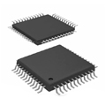
画像は参照用のみです。
EP1C3T144I7
IC FPGA 104 I/O 144TQFP
- メーカー
- Mfr。パート #EP1C3T144I7
- パッケージ 144-LQFP
- データシート
- 在庫中5697
100% オリジナル &新しい
出荷の準備ができている24時間
365日の保証
RFQおよびもっと割引を得る
仕様
| Package | Tray |
| Series | Cyclone® |
| ProductStatus | Obsolete |
| NumberofLABs/CLBs | 291 |
| NumberofLogicElements/Cells | 2910 |
| TotalRAMBits | 59904 |
| NumberofI/O | 104 |
| Voltage-Supply | 1.425V ~ 1.575V |
| MountingType | Surface Mount |
| OperatingTemperature | -40°C ~ 100°C (TJ) |
| Package/Case | 144-LQFP |
概要
Description
EP1C3T144I7 appears to be a coded or stylized term, possibly referring to a project, product, or concept that incorporates elements of technology, innovation, or digital culture. The alphanumeric structure suggests a blend of letters and numbers that could denote a unique identifier or model number.
In various contexts, such terms often relate to software, hardware, or specific methodologies in fields like programming, gaming, or digital art. If it pertains to a specific industry or domain, further clarification would be needed to provide detailed insights.
To understand its significance fully, consider exploring the context in which EP1C3T144I7 is used—such as a tech product launch, a software version, or a creative work. This will help pinpoint its relevance and applications.
In various contexts, such terms often relate to software, hardware, or specific methodologies in fields like programming, gaming, or digital art. If it pertains to a specific industry or domain, further clarification would be needed to provide detailed insights.
To understand its significance fully, consider exploring the context in which EP1C3T144I7 is used—such as a tech product launch, a software version, or a creative work. This will help pinpoint its relevance and applications.
Features
The EP1C3T144I7 is a member of the Altera (now Intel) EPIC series of programmable logic devices, specifically the MAX 3000 series. Key features include:
1. Logic Elements: Offers up to 144 logic elements, allowing for flexible design implementations.
2. Memory: Integrated memory blocks provide support for various memory configurations.
3. I/O Pins: Supports a wide range of I/O standards and configurations, enhancing connectivity.
4. Programmability: Configurable using hardware description languages (HDLs), enabling custom designs.
5. Power Efficiency: Designed for low power consumption, making it suitable for battery-operated devices.
6. Speed: Features fast switching speeds, which support high-performance applications.
7. Development Tools: Compatible with Intel's Quartus Prime software for straightforward design entry and optimization.
Overall, the EP1C3T144I7 is suitable for diverse applications, from consumer electronics to industrial automation, due to its versatility and performance.
1. Logic Elements: Offers up to 144 logic elements, allowing for flexible design implementations.
2. Memory: Integrated memory blocks provide support for various memory configurations.
3. I/O Pins: Supports a wide range of I/O standards and configurations, enhancing connectivity.
4. Programmability: Configurable using hardware description languages (HDLs), enabling custom designs.
5. Power Efficiency: Designed for low power consumption, making it suitable for battery-operated devices.
6. Speed: Features fast switching speeds, which support high-performance applications.
7. Development Tools: Compatible with Intel's Quartus Prime software for straightforward design entry and optimization.
Overall, the EP1C3T144I7 is suitable for diverse applications, from consumer electronics to industrial automation, due to its versatility and performance.
Package
The EP1C3T144I7 is packaged in a TQFP (Thin Quad Flat Package) format with 144 pins.
Pinout
The EP1C3T144I7 is a member of the Intel Cyclone I FPGA family. It features a pin count of 144.
The functions of the pins include:
- I/O Pins: Configurable for general-purpose input/output, supporting various I/O standards.
- Power Pins: For supplying core voltage and I/O voltage.
- Ground Pins: For electrical grounding.
- Configuration Pins: For programming and configuring the FPGA.
- Clock Pins: Dedicated pins for clock signals to ensure proper timing and synchronization.
- Serial and Parallel Communication Pins: For interfacing with other devices and protocols.
The specific functions of the pins can be configured during the design process using Intel’s Quartus Prime software, allowing designers to tailor the FPGA to their application needs.
The functions of the pins include:
- I/O Pins: Configurable for general-purpose input/output, supporting various I/O standards.
- Power Pins: For supplying core voltage and I/O voltage.
- Ground Pins: For electrical grounding.
- Configuration Pins: For programming and configuring the FPGA.
- Clock Pins: Dedicated pins for clock signals to ensure proper timing and synchronization.
- Serial and Parallel Communication Pins: For interfacing with other devices and protocols.
The specific functions of the pins can be configured during the design process using Intel’s Quartus Prime software, allowing designers to tailor the FPGA to their application needs.
Manufacturer
The EP1C3T144I7 is manufactured by Intel Corporation, specifically under its Altera product line, which focuses on field-programmable gate arrays (FPGAs) and related technologies. Intel is a multinational corporation based in the United States, primarily known for designing and manufacturing semiconductor products, including microprocessors, integrated circuits, and other hardware components. The company plays a crucial role in the computer and electronics industries, providing essential technologies for a wide range of applications, from consumer electronics to data center solutions. The EP1C3T144I7 is part of the Cyclone series of FPGAs, which are designed for cost-sensitive, low-power applications, making them suitable for various industries, including telecommunications, automotive, and industrial automation.
Application
The EP1C3T144I7 is a low-cost, low-power FPGA (Field-Programmable Gate Array) primarily used in embedded systems, industrial control, telecommunications, automotive applications, and digital signal processing. Its compact size and flexible architecture make it suitable for prototyping, data acquisition, and custom logic implementations in various electronic devices.
Equivalent
The EP1C3T144I7 chip is part of the Intel/Altera Cyclone I FPGA family. Equivalent products include the EP1C3T144C8 and EP1C3T144E7, which differ mainly in speed grade and temperature ranges. Other similar alternatives from different FPGA families or manufacturers may include low-cost options like Xilinx Spartan-6 or Lattice iCE40 series, depending on specific application requirements. Always verify pin compatibility and features for your needs.
出荷
出荷方法私たち
DHL、FedEx、TNT、UPS、またはあなたの選択の他の運送業者を通じてグローバルな出荷サービスを提供します。
出荷料参照(DHL/FedEx):
DHL の: 配送費は25ドル〜45ドル(0.5kg)の範囲で、推定配送時間は2〜5営業日です。
フェデックス: 配送費は25ドル〜40ドル(0.5kg)の範囲で、推定配送時間は3〜7営業日。
UPS の: 配送費は25ドル〜45ドル(0.5kg)の範囲で、推定配送時間は3〜7営業日。
TNT社: 配送費は25ドル〜65ドル(0.5kg)の範囲で、推定配送時間は3〜7営業日。
EMS: 配送料金は30〜50ドル(0.5kg)の範囲で、推定配送時間は7〜15営業日です。
登録航空郵便: 配送費は2〜4ドル(0.1kg)で、推定配送時間は5〜20営業日です。
支払い
Payment Methods
支払い期間は100%前払いです。
現在、下記の支払い方法のみを受け入れています。:
1. ペイパル
2. クレジット・デビットカード
3. ワイヤー 転送
類似
-
![MX25V5126FM1I]() MX25V5126FM1I
Macronix
-
![MX25V4035FZUI]() MX25V4035FZUI
Macronix
-
![MX25V2033FM1I]() MX25V2033FM1I
Macronix
-
![MX25V16066M1I02]() MX25V16066M1I02
Macronix
-
![MX25R3235FZNIL0]() MX25R3235FZNIL0
Macronix
-
![MX25V16066M2I02]() MX25V16066M2I02
Macronix
-
![MX25L8035EM2I-10G]() MX25L8035EM2I-10G
Macronix
-
![MX25U6435FM2I-10G]() MX25U6435FM2I-10G
Macronix
-
![MX25L12833FZ2I-10G]() MX25L12833FZ2I-10..
Macronix
-
![MX25L12833FZNI-10G]() MX25L12833FZNI-10..
Macronix
-
![MX25L25645GXDI-08G]() MX25L25645GXDI-08..
Macronix
-
![MX30LF4G18AC-TI]() MX30LF4G18AC-TI
Macronix