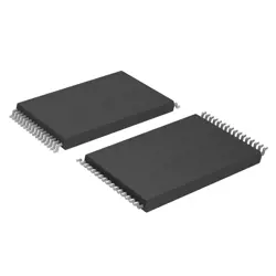
画像は参照用のみです。
DA14581-00AT2
IC RF TXRX+MCU BLE 40QFN
- メーカー
- Mfr。パート #DA14581-00AT2
- パッケージ
- データシート
- 在庫中3521
100% オリジナル &新しい
出荷の準備ができている24時間
365日の保証
RFQおよびもっと割引を得る
仕様
| Part Status | Not For New Designs |
| DigiKey Programmable | Not Verified |
| Type | TxRx + MCU |
| RF Family/Standard | Bluetooth |
| Protocol | Bluetooth v4.1 |
| Frequency | 2.4GHz |
| Power - Output | -1dBm |
| Sensitivity | -93dBm |
| Memory Size | 32kB OTP, 84kB ROM, 50kB SRAM |
| Serial Interfaces | I2C, SPI, UART |
| GPIO | 24 |
| Voltage - Supply | 2.35V ~ 3.3V |
| Current - Receiving | 3.7mA |
| Current - Transmitting | 3.4mA |
| Operating Temperature | -40°C ~ 85°C |
| Mounting Type | Surface Mount |
| Package / Case | 40-VFQFN Exposed Pad |
| Supplier Device Package | 40-QFN (5x5) |
| Base Product Number | DA14581 |
概要
Description
The DA14581-00AT2 is a low-power Bluetooth Smart (Bluetooth Low Energy) System-on-Chip (SoC) designed by Dialog Semiconductor, now part of Renesas Electronics. It is targeted for applications in the Internet of Things (IoT), wearables, and other smart devices that require efficient power consumption and compact size. The SoC integrates a Bluetooth 4.2 controller and host, alongside an ARM Cortex-M0 processor, which allows for efficient handling of Bluetooth communication and application tasks.
Key features of the DA14581 include its low energy consumption, which extends battery life in portable devices, and its small footprint, making it suitable for compact designs. It supports a range of peripherals and interfaces, such as UART, SPI, I2C, and GPIOs, enabling versatile connectivity options for developers. The chip also offers robust security features, including AES-128 encryption and Bluetooth Smart security modes.
The DA14581 is supported by a comprehensive development environment, including software development kits (SDKs) and reference designs, which facilitate the development process and accelerate time-to-market for Bluetooth-enabled products.
Features
The DA14581-00AT2 is a Bluetooth low energy (BLE) system-on-chip (SoC) designed for low-power wireless applications. Key features include:
1. BLE Support: It supports Bluetooth 4.2, offering enhanced connectivity and data transfer capabilities.
2. Ultra-Low Power Consumption: Optimized for low energy usage, the DA14581 is ideal for battery-powered devices, extending battery life significantly.
3. Integrated ARM Cortex-M0 Processor: Provides efficient processing power for various applications while maintaining low power consumption.
4. Flexible Memory: Incorporates SRAM and One-Time Programmable (OTP) memory for firmware and data storage, allowing for customizable applications.
5. Advanced Security: Features AES-128 encryption to ensure secure data transmission over Bluetooth connections.
6. Peripheral Interfaces: Includes UART, SPI, I2C, and GPIOs, enabling integration with a variety of sensors and external devices.
7. Small Form Factor: With its compact design, it is suitable for space-constrained applications such as wearable devices and IoT projects.
8. Development Support: Supported by a comprehensive development kit and software development environment, facilitating rapid prototyping and deployment.
These features make the DA14581-00AT2 an excellent choice for developing efficient, secure, and compact wireless solutions.
Package
The DA14581-00AT2 is a Bluetooth Low Energy (BLE) system-on-chip (SoC) designed by Dialog Semiconductor. It is typically available in a QFN (Quad Flat No-leads) package type, which is compact and suitable for space-constrained applications.
Pinout
The DA14581-00AT2 is a Bluetooth Low Energy (BLE) System-on-Chip (SoC) developed by Dialog Semiconductor. It is designed for low-power wireless communication applications. The chip comes in a compact package with a specific pin count, which is crucial for its functionality and integration into various devices.
The DA14581-00AT2 typically comes in a 32-pin QFN (Quad Flat No-leads) package. These pins are used for various purposes, including power supply, ground, analog and digital I/O, and specific functionalities such as UART, SPI, I2C interfaces, and GPIOs (General Purpose Input/Output). The pin configuration supports the integration of additional peripherals and external components, which can be essential for developing custom applications.
This SoC is particularly suitable for wearable devices, smart home applications, and other IoT devices that require efficient Bluetooth connectivity with low power consumption. The combination of its pin count and integrated features makes it versatile for developers aiming to implement BLE into their products.
Manufacturer
The DA14581-00AT2 is manufactured by Dialog Semiconductor. Dialog Semiconductor is a company specializing in the development of highly integrated mixed-signal integrated circuits (ICs) for consumer electronics, automotive, computing, and industrial applications. They are known for providing solutions in power management, audio, charging, Bluetooth low energy technology, and other connectivity solutions. The company's products are used in various devices such as smartphones, tablets, and other portable devices. Dialog Semiconductor is recognized for its focus on energy-efficient technologies and plays a significant role in the semiconductor industry.
Application
The DA14581-00AT2 is a Bluetooth Low Energy (BLE) System-on-Chip (SoC) designed for low-power wireless communication. It is commonly used in application areas such as wearable devices, smart home products, health and fitness devices, remote controls, and Internet of Things (IoT) devices. Its low power consumption and compact size make it suitable for battery-operated products requiring reliable BLE connectivity.
Equivalent
The DA14581-00AT2 is a Bluetooth Low Energy (BLE) System-on-Chip (SoC) from Renesas (formerly Dialog Semiconductor). Equivalent products include Nordic Semiconductor's nRF51/nRF52 series, Texas Instruments' CC2540/CC2640 series, Silicon Labs' EFR32BG series, and Microchip's RN4020. These alternatives offer similar BLE functionality and support various applications in wireless communication. Consider specific requirements like power consumption, processing capabilities, and peripheral support when choosing an equivalent.
出荷
出荷方法私たち
DHL、FedEx、TNT、UPS、またはあなたの選択の他の運送業者を通じてグローバルな出荷サービスを提供します。
出荷料参照(DHL/FedEx):
DHL の: 配送費は25ドル〜45ドル(0.5kg)の範囲で、推定配送時間は2〜5営業日です。
フェデックス: 配送費は25ドル〜40ドル(0.5kg)の範囲で、推定配送時間は3〜7営業日。
UPS の: 配送費は25ドル〜45ドル(0.5kg)の範囲で、推定配送時間は3〜7営業日。
TNT社: 配送費は25ドル〜65ドル(0.5kg)の範囲で、推定配送時間は3〜7営業日。
EMS: 配送料金は30〜50ドル(0.5kg)の範囲で、推定配送時間は7〜15営業日です。
登録航空郵便: 配送費は2〜4ドル(0.1kg)で、推定配送時間は5〜20営業日です。
支払い
Payment Methods
支払い期間は100%前払いです。
現在、下記の支払い方法のみを受け入れています。:
1. ペイパル
2. クレジット・デビットカード
3. ワイヤー 転送
類似
-
![MX25L3233FZBI-08Q]() MX25L3233FZBI-08Q
Macronix
-
![MX25V1635FZNQ03]() MX25V1635FZNQ03
Macronix
-
![MX25V5126FM1I]() MX25V5126FM1I
Macronix
-
![MX25V4035FZUI]() MX25V4035FZUI
Macronix
-
![MX25V16066M2I02]() MX25V16066M2I02
Macronix
-
![MX29GL512FHXFI-11G]() MX29GL512FHXFI-11..
Macronix
-
![MX25V1635FM2I]() MX25V1635FM2I
Macronix
-
![MX25U3232FZBI02]() MX25U3232FZBI02
Macronix
-
![MX25L6433FM2I-08G]() MX25L6433FM2I-08G
Macronix
-
![MX25L12833FM2I-10G]() MX25L12833FM2I-10..
Macronix
-
![MX29F040CQI-70G]() MX29F040CQI-70G
Macronix
-
![MX29F040CTI-70G]() MX29F040CTI-70G
Macronix