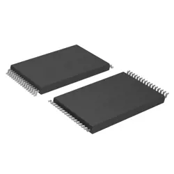
画像は参照用のみです。
CDCV304PWR
IC CLK BUFFER 1:4 200MHZ 8TSSOP
- メーカー
- Mfr。パート #CDCV304PWR
- パッケージ TSSOP (PW)-8
- データシート
- 在庫中4956
100% オリジナル &新しい
出荷の準備ができている24時間
365日の保証
RFQおよびもっと割引を得る
仕様
| Package | Tape & Reel (TR),Cut Tape (CT),Bulk |
| ProductStatus | Active |
| Type | Fanout Buffer (Distribution) |
| NumberofCircuits | 1 |
| Ratio-Input:Output | 1:4 |
| Differential-Input:Output | No/No |
| Input | LVTTL |
| Output | LVTTL |
| Frequency-Max | 200 MHz |
| Voltage-Supply | 2.3V ~ 3.6V |
| OperatingTemperature | -40°C ~ 85°C |
| MountingType | Surface Mount |
| Package/Case | 8-TSSOP (0.173, 4.40mm Width) |
概要
Description
CDCV304PWR is likely a reference to a specific course or program, possibly within a curriculum related to power electronics, control systems, or a similar field. The acronym CDCV might denote "Control Design and Circuit Validation," while "304" could indicate the course code, and "PWR" may refer to power systems or power electronics.
In such a course, students typically learn about the principles of designing and validating control systems for power applications. Topics may include control theory, system dynamics, circuit design, modeling, simulation, and implementation. Emphasis is often placed on practical applications, including renewable energy systems, electric drives, and automation technologies.
Students might engage in hands-on projects, simulations, and labs to apply theoretical knowledge to real-world scenarios, preparing them for careers in engineering, research, or related fields. Ultimately, the course aims to equip students with the skills needed to design efficient and reliable power systems.
Features
The CDCV304PWR is a low-power, quad differential line driver and receiver designed for high-speed communication. Key features include:
1. Quad Configuration: Contains four differential pairs, enabling multiple data channels.
2. High Data Rate: Supports data rates up to 1 Gbps, making it suitable for fast data transmission.
3. Low Power Consumption: Operates with low quiescent current, enhancing energy efficiency for battery-operated devices.
4. Wide Voltage Range: Compatible with a wide supply voltage range, typically from 3.0V to 5.5V.
5. High Noise Immunity: Differential signaling reduces susceptibility to electromagnetic interference, improving signal integrity.
6. Integrated Termination: Built-in termination resistors simplify board design and improve performance.
7. Temperature Range: Operates within a broad temperature range, suitable for various environmental conditions.
8. Small Package Size: Available in compact packages, facilitating integration into space-constrained applications.
These features make the CDCV304PWR ideal for applications in telecommunications, data communications, and consumer electronics.
Package
The CDCV304PWR is packaged in a TQFP (Thin Quad Flat Package) format, specifically a 32-pin TQFP. This package type is designed for surface mounting and provides a low-profile solution suitable for various applications.
Pinout
The CDCV304PWR is a clock distribution IC with a pin count of 16. Its primary function is to distribute a single clock input to multiple clock outputs while maintaining signal integrity and minimizing skew.
Key features include:
- Four low-skew clock outputs
- Support for differential and single-ended input clock signals
- Selectable output frequencies
- Integrated output buffers for improved drive capability
The device is commonly used in applications where a stable clock signal is required, such as in telecommunications, data communications, and high-speed digital systems. It operates over a wide voltage range and offers features such as power-down modes to enhance efficiency.
Manufacturer
The CDCV304PWR is manufactured by Texas Instruments (TI), a well-known American technology company. Texas Instruments specializes in the design and production of semiconductor products and various integrated circuits, including analog and mixed-signal devices, digital signal processors (DSPs), and microcontrollers. Founded in 1930, TI is recognized for its innovations in the electronics industry and serves a diverse range of markets, including automotive, industrial, personal electronics, and communication equipment. The company is also notable for its role in developing calculators and educational technology. With a strong focus on research and development, Texas Instruments continues to be a leading player in the global semiconductor market.
Application
The CDCV304PWR is a dual-channel, low-power, high-speed clock driver used in various applications including networking (switches and routers), telecommunications, data communications, and high-speed interfaces. It enhances signal integrity in clock distribution systems, supports multi-channel synchronization, and is suitable for high-frequency designs in consumer electronics, automotive systems, and industrial automation.
Equivalent
The CDCV304PWR is a clock buffer and driver. Equivalent products include the Texas Instruments CDCV304, NXP NX3DV304, and ON Semiconductor MC100LVEL16. Always verify the specific application requirements and specifications when considering substitutes.
出荷
出荷方法私たち
DHL、FedEx、TNT、UPS、またはあなたの選択の他の運送業者を通じてグローバルな出荷サービスを提供します。
出荷料参照(DHL/FedEx):
DHL の: 配送費は25ドル〜45ドル(0.5kg)の範囲で、推定配送時間は2〜5営業日です。
フェデックス: 配送費は25ドル〜40ドル(0.5kg)の範囲で、推定配送時間は3〜7営業日。
UPS の: 配送費は25ドル〜45ドル(0.5kg)の範囲で、推定配送時間は3〜7営業日。
TNT社: 配送費は25ドル〜65ドル(0.5kg)の範囲で、推定配送時間は3〜7営業日。
EMS: 配送料金は30〜50ドル(0.5kg)の範囲で、推定配送時間は7〜15営業日です。
登録航空郵便: 配送費は2〜4ドル(0.1kg)で、推定配送時間は5〜20営業日です。
支払い
Payment Methods
支払い期間は100%前払いです。
現在、下記の支払い方法のみを受け入れています。:
1. ペイパル
2. クレジット・デビットカード
3. ワイヤー 転送
類似
-
![MX25V1635FZNI]() MX25V1635FZNI
Macronix
-
![MX25V5126FM1I]() MX25V5126FM1I
Macronix
-
![MX25V2033FM1I]() MX25V2033FM1I
Macronix
-
![MX25R3235FZNIL0]() MX25R3235FZNIL0
Macronix
-
![MX25V16066M2I02]() MX25V16066M2I02
Macronix
-
![MX25L2006EM1I-12G]() MX25L2006EM1I-12G
Macronix
-
![MX25U6435FM2I-10G]() MX25U6435FM2I-10G
Macronix
-
![MX25U25645GXDI00]() MX25U25645GXDI00
Macronix
-
![MX25L12835FZ2I-10G]() MX25L12835FZ2I-10..
Macronix
-
![MX29F040CQI-70G]() MX29F040CQI-70G
Macronix
-
![MX25L25645GXDI-08G]() MX25L25645GXDI-08..
Macronix
-
![MX29F040CTI-70G]() MX29F040CTI-70G
Macronix