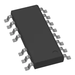
画像は参照用のみです。
CDCS503PWR
IC CLK BUFFER 1:1 108MHZ 8TSSOP
- メーカー
- Mfr。パート #CDCS503PWR
- パッケージ TSSOP (PW)-8
- データシート
- 在庫中7161
100% オリジナル &新しい
出荷の準備ができている24時間
365日の保証
RFQおよびもっと割引を得る
仕様
| Package | Tape & Reel (TR),Cut Tape (CT),Bulk |
| ProductStatus | Active |
| Type | Buffer/Driver, Multiplier |
| NumberofCircuits | 1 |
| Ratio-Input:Output | 1:1 |
| Differential-Input:Output | No/No |
| Input | LVCMOS |
| Output | LVCMOS |
| Frequency-Max | 108 MHz |
| Voltage-Supply | 3V ~ 3.6V |
| OperatingTemperature | -40°C ~ 85°C |
| MountingType | Surface Mount |
| Package/Case | 8-TSSOP (0.173, 4.40mm Width) |
概要
Description
CDCS503PWR is a course focused on advanced concepts in power systems and control. It typically covers key topics such as power flow analysis, stability, control strategies, and the integration of renewable energy sources. Students explore both theoretical foundations and practical applications, gaining insights into modern power system challenges, including grid reliability and efficiency. The curriculum may also include simulations and case studies to enhance understanding. This course is essential for those pursuing careers in electrical engineering, energy management, and related fields, equipping them with the skills necessary to design, analyze, and manage complex power systems effectively.
Features
The CDCS503PWR is a versatile power management IC designed for various applications, including battery-powered devices and consumer electronics. Key features include:
1. High Efficiency: It offers efficient power conversion, minimizing energy loss and extending battery life.
2. Multiple Outputs: Supports multiple output voltages, allowing for flexible system design.
3. Integrated Protection: Features overcurrent and thermal protection to ensure reliability and safety.
4. Adjustable Output Voltage: Users can configure the output voltage as needed for specific applications.
5. Compact Package: The small form factor makes it suitable for space-constrained designs.
6. Low Quiescent Current: Ensures minimal power draw in standby mode, enhancing battery performance.
7. Wide Input Voltage Range: Accommodates a broad range of input voltages for various power sources.
These features make the CDCS503PWR a robust choice for engineers looking to optimize power management in their designs.
Package
The CDCS503PWR is available in a 16-pin TSSOP (Thin Shrink Small Outline Package) package type.
Pinout
The CDCS503PWR is a programmable clock generator from Texas Instruments. It features a total of 28 pins. The primary functions include generating multiple clock outputs and allowing for adjustable frequencies and phase settings.
Key pin functions include:
- XTAL1/XTAL2: Crystal oscillator connections for external frequency reference.
- CLKOUT0 to CLKOUT4: Clock output pins that provide various clock signals.
- NSEL: Selects the clock output source.
- ENABLE: Activates the device.
- I2C pins (SDA, SCL): For serial communication to configure settings.
- GND/VCC: Power supply and ground connections.
The device is designed for applications requiring precise clock generation, such as in communications, consumer electronics, and data processing systems.
Manufacturer
The CDCS503PWR is manufactured by Texas Instruments (TI), a well-established American technology company. Texas Instruments specializes in the design and production of semiconductors and various integrated circuits. They are particularly renowned for their innovation in analog electronics, embedded processing, and digital signal processing. The company serves a wide range of markets, including automotive, industrial, communications, and consumer electronics, contributing to various applications such as power management, signal processing, and connectivity solutions. Established in 1930, TI continues to be a leading player in the semiconductor industry, focusing on advancing technology to improve performance and efficiency in electronic devices.
Application
CDCS503PWR is commonly used in various application areas such as power management systems, industrial automation, renewable energy systems, electric vehicles, and consumer electronics. It is designed for efficient power conversion, voltage regulation, and energy storage management, facilitating improved performance and reliability in these sectors.
Equivalent
The CDCS503PWR is a clock generator IC. Equivalent products include the CDCS520, CDCS521, and CDCS510, which offer similar functionalities. For specific applications, other brands like the Si5351 from Silicon Labs and the LMK04828 from Texas Instruments may also serve as alternatives, depending on the required specifications such as frequency range and output type. Always verify compatibility with your circuit requirements.
出荷
出荷方法私たち
DHL、FedEx、TNT、UPS、またはあなたの選択の他の運送業者を通じてグローバルな出荷サービスを提供します。
出荷料参照(DHL/FedEx):
DHL の: 配送費は25ドル〜45ドル(0.5kg)の範囲で、推定配送時間は2〜5営業日です。
フェデックス: 配送費は25ドル〜40ドル(0.5kg)の範囲で、推定配送時間は3〜7営業日。
UPS の: 配送費は25ドル〜45ドル(0.5kg)の範囲で、推定配送時間は3〜7営業日。
TNT社: 配送費は25ドル〜65ドル(0.5kg)の範囲で、推定配送時間は3〜7営業日。
EMS: 配送料金は30〜50ドル(0.5kg)の範囲で、推定配送時間は7〜15営業日です。
登録航空郵便: 配送費は2〜4ドル(0.1kg)で、推定配送時間は5〜20営業日です。
支払い
Payment Methods
支払い期間は100%前払いです。
現在、下記の支払い方法のみを受け入れています。:
1. ペイパル
2. クレジット・デビットカード
3. ワイヤー 転送
類似
-
![MX66U1G45GXDI00]() MX66U1G45GXDI00
Macronix
-
![MX25R3235FZNIL0]() MX25R3235FZNIL0
Macronix
-
![MX29GL512FHXFI-11G]() MX29GL512FHXFI-11..
Macronix
-
![MX25L2006EM1I-12G]() MX25L2006EM1I-12G
Macronix
-
![MX25U3232FZBI02]() MX25U3232FZBI02
Macronix
-
![MX25L6433FM2I-08G]() MX25L6433FM2I-08G
Macronix
-
![MX25U6435FM2I-10G]() MX25U6435FM2I-10G
Macronix
-
![MX25L12835FZ2I-10G]() MX25L12835FZ2I-10..
Macronix
-
![MX29LV160DTTI-70G]() MX29LV160DTTI-70G
Macronix
-
![MX25L25735FMI-10G]() MX25L25735FMI-10G
Macronix
-
![MX30LF4G18AC-TI]() MX30LF4G18AC-TI
Macronix
-
![MX25L1006EMI-10G]() MX25L1006EMI-10G
Macronix