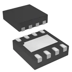
画像は参照用のみです。
CDCE62002RHBR
IC CLOCK GENERATOR 32VQFN
- メーカー
- Mfr。パート #CDCE62002RHBR
- パッケージ
- データシート
- 在庫中4586
100% オリジナル &新しい
出荷の準備ができている24時間
365日の保証
RFQおよびもっと割引を得る
仕様
| Part Status | Active |
| DigiKey Programmable | Not Verified |
| Type | Clock Generator |
| PLL | Yes |
| Input | LVCMOS, LVDS, LVPECL, Crystal |
| Output | LVCMOS, LVDS, LVPECL |
| Number of Circuits | 1 |
| Ratio - Input:Output | 2:2 |
| Differential - Input:Output | Yes/Yes |
| Frequency - Max | 1.175GHz |
| Divider/Multiplier | Yes/No |
| Voltage - Supply | 3V ~ 3.6V |
| Operating Temperature | -40°C ~ 85°C |
| Mounting Type | Surface Mount |
| Package / Case | 32-VFQFN Exposed Pad |
| Supplier Device Package | 32-VQFN (5x5) |
| Base Product Number | CDCE62002 |
概要
Description
CDCE62002RHBR is a high-performance, programmable clock generator and frequency synthesizer designed for various applications, including telecommunications, data centers, and consumer electronics. It operates within a wide frequency range and can generate multiple output frequencies from a single input reference clock. The device features low phase noise and high stability, making it suitable for precision timing applications.
Key characteristics include the ability to program output frequencies, support for differential and single-ended outputs, and various output formats. Additionally, it offers integrated power management features, allowing for efficient operation and reducing power consumption. The CDCE62002RHBR is designed for easy integration into systems, with an I2C interface for configuration and control.
Overall, this component is essential for applications requiring high-frequency precision and flexibility in clock management.
Key characteristics include the ability to program output frequencies, support for differential and single-ended outputs, and various output formats. Additionally, it offers integrated power management features, allowing for efficient operation and reducing power consumption. The CDCE62002RHBR is designed for easy integration into systems, with an I2C interface for configuration and control.
Overall, this component is essential for applications requiring high-frequency precision and flexibility in clock management.
Features
The CDCE62002RHBR is a high-performance clock buffer and fanout driver designed for use in various applications, including data communications and networking. Key features include:
1. Low Jitter Performance: Ensures high signal integrity with minimal phase noise.
2. Multiple Outputs: Offers multiple buffered clock outputs, typically up to 2.
3. Wide Frequency Range: Capable of handling a broad frequency range, which allows it to support various clock sources.
4. Input Compatibility: Accepts a variety of input signal types, providing flexibility in system design.
5. Power Supply Options: Operates on low voltage (typically 3.3V), promoting energy efficiency.
6. Applications: Ideal for use in high-speed communication systems, such as Ethernet and PCIe.
7. Thermal and Electrical Performance: Designed for minimal heat generation and reliable operation under various conditions.
This device is suitable for applications where precise clock management is crucial.
1. Low Jitter Performance: Ensures high signal integrity with minimal phase noise.
2. Multiple Outputs: Offers multiple buffered clock outputs, typically up to 2.
3. Wide Frequency Range: Capable of handling a broad frequency range, which allows it to support various clock sources.
4. Input Compatibility: Accepts a variety of input signal types, providing flexibility in system design.
5. Power Supply Options: Operates on low voltage (typically 3.3V), promoting energy efficiency.
6. Applications: Ideal for use in high-speed communication systems, such as Ethernet and PCIe.
7. Thermal and Electrical Performance: Designed for minimal heat generation and reliable operation under various conditions.
This device is suitable for applications where precise clock management is crucial.
Package
The CDCE62002RHBR is packaged in a 48-pin HTQFP (Thin Quad Flat Package) format. This type of package is designed for surface mounting and is characterized by its thin profile and lead arrangement, suitable for high-density applications.
Pinout
The CDCE62002RHBR is a clock generator and frequency synthesizer from Texas Instruments. It has a total of 20 pins.
Pin Functions:
1. Power and Ground Pins:
- VDD: Supply voltage
- GND: Ground
2. Input Pins:
- XTAL1, XTAL2: Crystal oscillator connections for specifying the reference frequency.
- REFCLK: External reference clock input.
3. Output Pins:
- CLKOUT0 - CLKOUT5: Multiple clock output signals with programmable frequency and duty cycle.
4. Configuration Pins:
- I2C: SDA, SCL pins for serial data communication for configuration.
- /RESET: Active low reset pin.
- /S0, /S1: Select pins for mode selection.
5. Status Pins:
- LOCK: Indicates the lock status of the PLL.
This device is designed for applications requiring precise clock generation with reduced jitter and flexibility in frequency settings.
Pin Functions:
1. Power and Ground Pins:
- VDD: Supply voltage
- GND: Ground
2. Input Pins:
- XTAL1, XTAL2: Crystal oscillator connections for specifying the reference frequency.
- REFCLK: External reference clock input.
3. Output Pins:
- CLKOUT0 - CLKOUT5: Multiple clock output signals with programmable frequency and duty cycle.
4. Configuration Pins:
- I2C: SDA, SCL pins for serial data communication for configuration.
- /RESET: Active low reset pin.
- /S0, /S1: Select pins for mode selection.
5. Status Pins:
- LOCK: Indicates the lock status of the PLL.
This device is designed for applications requiring precise clock generation with reduced jitter and flexibility in frequency settings.
Manufacturer
The CDCE62002RHBR is manufactured by Texas Instruments (TI), a global semiconductor company. Texas Instruments designs and produces a wide range of electronic components, including analog and digital semiconductors, microcontrollers, and processors. Established in 1930, TI is known for its innovation in the field of electronics and serves various markets, including automotive, industrial, communication, and consumer electronics. The CDCE62002 is a programmable clock generator that provides multiple output clocks and is used in applications requiring precise timing solutions.
Application
The CDCE62002RHBR is a clock generator and fanout buffer used primarily in high-performance applications such as telecommunications, data communications, and networking. Its application areas include optical networking, server and storage systems, and high-speed data converters, where precise clocking is essential for synchronization and signal integrity. It supports multiple output frequencies and clock distribution, making it suitable for complex electronic systems requiring reliable timing solutions.
Equivalent
The CDCE62002RHBR can be replaced by similar clock generators and frequency synthesizers such as the Texas Instruments CDCE62005, CDCE62003, or the Si5351 from Silicon Labs. Ensure to verify specifications like frequency range, output type, and pin compatibility before substituting. Always refer to the manufacturer's data sheets for detailed information.
出荷
出荷方法私たち
DHL、FedEx、TNT、UPS、またはあなたの選択の他の運送業者を通じてグローバルな出荷サービスを提供します。
出荷料参照(DHL/FedEx):
DHL の: 配送費は25ドル〜45ドル(0.5kg)の範囲で、推定配送時間は2〜5営業日です。
フェデックス: 配送費は25ドル〜40ドル(0.5kg)の範囲で、推定配送時間は3〜7営業日。
UPS の: 配送費は25ドル〜45ドル(0.5kg)の範囲で、推定配送時間は3〜7営業日。
TNT社: 配送費は25ドル〜65ドル(0.5kg)の範囲で、推定配送時間は3〜7営業日。
EMS: 配送料金は30〜50ドル(0.5kg)の範囲で、推定配送時間は7〜15営業日です。
登録航空郵便: 配送費は2〜4ドル(0.1kg)で、推定配送時間は5〜20営業日です。
支払い
Payment Methods
支払い期間は100%前払いです。
現在、下記の支払い方法のみを受け入れています。:
1. ペイパル
2. クレジット・デビットカード
3. ワイヤー 転送
類似
-
![MX25R8035FM1IL0]() MX25R8035FM1IL0
Macronix
-
![MX25L3233FM1I-08Q]() MX25L3233FM1I-08Q
Macronix
-
![MX25V1635FZNI]() MX25V1635FZNI
Macronix
-
![MX29F400CBTI-70G]() MX29F400CBTI-70G
Macronix
-
![MX25V5126FM1I]() MX25V5126FM1I
Macronix
-
![MX25V2033FM1I]() MX25V2033FM1I
Macronix
-
![MX25R6435FBDIL0]() MX25R6435FBDIL0
Macronix
-
![MX29GL512FHXFI-11G]() MX29GL512FHXFI-11..
Macronix
-
![MX25L2006EM1I-12G]() MX25L2006EM1I-12G
Macronix
-
![MX25R1635FZUIH0]() MX25R1635FZUIH0
Macronix
-
![MX25V1635FM2I]() MX25V1635FM2I
Macronix
-
![MX25L6433FM2I-08G]() MX25L6433FM2I-08G
Macronix