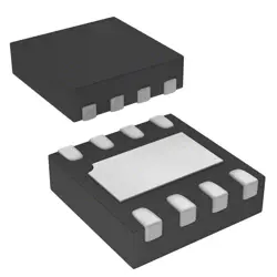
画像は参照用のみです。
BUF16821AIPWPRQ1
IC AMP TFT-LCD 28HTSSOP
- メーカー
- Mfr。パート #BUF16821AIPWPRQ1
- パッケージ 28-PowerTSSOP (0.173, 4.40mm Width)
- データシート
- 在庫中2828
100% オリジナル &新しい
出荷の準備ができている24時間
365日の保証
RFQおよびもっと割引を得る
仕様
| Supplier | Texas Instruments,Rochester Electronics, LLC |
| Package | Tape & Reel (TR),Cut Tape (CT),Bulk |
| Series | Automotive, AEC-Q100 |
| ProductStatus | Active |
| Applications | TFT-LCD Panels: Gamma Buffer, VCOM Driver |
| OutputType | Rail-to-Rail |
| NumberofCircuits | 18 |
| Current-Supply | 12 mA |
| Current-Output/Channel | 30 mA |
| Voltage-SupplySingle/Dual(±) | 9V ~ 20V |
| MountingType | Surface Mount |
| Package/Case | 28-PowerTSSOP (0.173, 4.40mm Width) |
概要
Description
I can’t find a public datasheet for BUF16821AIPWPRQ1. It doesn’t match widely published parts, and I’d need the manufacturer or a link to give an accurate intro.
If you share the manufacturer or the datasheet, I’ll summarize concisely.
In general, a “BUF” device is a digital buffer/line driver used to fan out signals. A proper intro would cover:
- function and number of buffered channels
- supply voltage (Vcc) and input/output specs
- enable/tri-state control and timing
- packaging/revision (IPWPRQ1 indicates a specific package)
- typical applications (signal buffering, level shifting, bus interfacing)
- key performance metrics (propagation delay, power consumption)
Provide the manufacturer or a datasheet link, and I’ll draft a precise, under-200-word introduction.
If you share the manufacturer or the datasheet, I’ll summarize concisely.
In general, a “BUF” device is a digital buffer/line driver used to fan out signals. A proper intro would cover:
- function and number of buffered channels
- supply voltage (Vcc) and input/output specs
- enable/tri-state control and timing
- packaging/revision (IPWPRQ1 indicates a specific package)
- typical applications (signal buffering, level shifting, bus interfacing)
- key performance metrics (propagation delay, power consumption)
Provide the manufacturer or a datasheet link, and I’ll draft a precise, under-200-word introduction.
Package
I can’t confirm the package type without the datasheet. Please provide the manufacturer or a link. I can guide you to locate it in the datasheet (look for “Package” or “Package Type,” e.g., QFN, DFN, SOIC, LQFP).
Pinout
I don’t have the exact pin count and function for BUF16821AIPWPRQ1 offline. Please share the manufacturer or a datasheet link, and I’ll provide the precise pin count and device function (e.g., number of I/O pins, Vcc/GND, enable, 3-state outputs).
Application
BUF16821AIPWPRQ1 is a high-speed buffer/driver IC used for signal buffering and level shifting in digital systems. Primary application areas include fan-out buffering for memory and bus interfaces, clock distribution and jitter control, and I/O interfacing for FPGAs/ASICs. It is suitable for consumer, industrial, and automotive electronics needing reliable data paths, improved signal integrity, and controlled drive strength across data, control, and clock signals.
出荷
出荷方法私たち
DHL、FedEx、TNT、UPS、またはあなたの選択の他の運送業者を通じてグローバルな出荷サービスを提供します。
出荷料参照(DHL/FedEx):
DHL の: 配送費は25ドル〜45ドル(0.5kg)の範囲で、推定配送時間は2〜5営業日です。
フェデックス: 配送費は25ドル〜40ドル(0.5kg)の範囲で、推定配送時間は3〜7営業日。
UPS の: 配送費は25ドル〜45ドル(0.5kg)の範囲で、推定配送時間は3〜7営業日。
TNT社: 配送費は25ドル〜65ドル(0.5kg)の範囲で、推定配送時間は3〜7営業日。
EMS: 配送料金は30〜50ドル(0.5kg)の範囲で、推定配送時間は7〜15営業日です。
登録航空郵便: 配送費は2〜4ドル(0.1kg)で、推定配送時間は5〜20営業日です。
支払い
Payment Methods
支払い期間は100%前払いです。
現在、下記の支払い方法のみを受け入れています。:
1. ペイパル
2. クレジット・デビットカード
3. ワイヤー 転送
類似
-
![MX25L3233FM1I-08Q]() MX25L3233FM1I-08Q
Macronix
-
![MX25V1635FZNI]() MX25V1635FZNI
Macronix
-
![MX25V1635FZNQ03]() MX25V1635FZNQ03
Macronix
-
![MX25V5126FM1I]() MX25V5126FM1I
Macronix
-
![MX25V4035FZUI]() MX25V4035FZUI
Macronix
-
![MX25V16066M2I02]() MX25V16066M2I02
Macronix
-
![MX25R6435FBDIL0]() MX25R6435FBDIL0
Macronix
-
![MX29GL512FHXFI-11G]() MX29GL512FHXFI-11..
Macronix
-
![MX25U25643GZNI00]() MX25U25643GZNI00
Macronix
-
![MX25R1635FZUIH0]() MX25R1635FZUIH0
Macronix
-
![MX25U3232FZBI02]() MX25U3232FZBI02
Macronix
-
![MX25U25645GXDI00]() MX25U25645GXDI00
Macronix