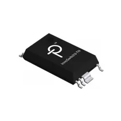
画像は参照用のみです。
BSS83PH6327XTSA1
MOSFET P-CH 60V 330MA SOT23-3
- メーカー
- Mfr。パート #BSS83PH6327XTSA1
- パッケージ PG-SOT23-3
- データシート
- 在庫中2072
100% オリジナル &新しい
出荷の準備ができている24時間
365日の保証
RFQおよびもっと割引を得る
仕様
| Package | Tape & Reel (TR),Cut Tape (CT) |
| Series | SIPMOS® |
| ProductStatus | Active |
| FETType | P-Channel |
| Technology | MOSFET (Metal Oxide) |
| DraintoSourceVoltage(Vdss) | 60 V |
| Current-ContinuousDrain(Id)@25°C | 330mA (Ta) |
| DriveVoltage(MaxRdsOnMinRdsOn) | 4.5V, 10V |
| RdsOn(Max)@IdVgs | 2Ohm @ 330mA, 10V |
| Vgs(th)(Max)@Id | 2V @ 80µA |
| GateCharge(Qg)(Max)@Vgs | 3.57 nC @ 10 V |
| Vgs(Max) | ±20V |
| InputCapacitance(Ciss)(Max)@Vds | 78 pF @ 25 V |
| PowerDissipation(Max) | 360mW (Ta) |
| OperatingTemperature | -55°C ~ 150°C (TJ) |
| MountingType | Surface Mount |
| SupplierDevicePackage | PG-SOT23 |
概要
Description
BSS83PH6327XTSA1 is a specific type of MOSFET (Metal-Oxide-Semiconductor Field-Effect Transistor) designed for low-voltage applications. It is an N-channel MOSFET known for its low on-resistance and fast switching capabilities, making it suitable for various electronic devices, including power management circuits, switching applications, and signal routing.
Key specifications often include a maximum drain-source voltage (V_DS), typically around 60V, and a continuous drain current (I_D) rating, which allows it to handle moderate power levels efficiently. Its compact surface-mount package (often in SOT-23 or similar) facilitates easy integration into printed circuit boards (PCBs).
When using the BSS83PH6327XTSA1, it is essential to consider the thermal characteristics and ensure proper heat dissipation to avoid performance degradation. Its reliability and efficiency make it a popular choice among engineers for enhancing circuit performance in consumer electronics and industrial applications. Always refer to the manufacturer's datasheet for detailed specifications and guidelines for optimal usage.
Key specifications often include a maximum drain-source voltage (V_DS), typically around 60V, and a continuous drain current (I_D) rating, which allows it to handle moderate power levels efficiently. Its compact surface-mount package (often in SOT-23 or similar) facilitates easy integration into printed circuit boards (PCBs).
When using the BSS83PH6327XTSA1, it is essential to consider the thermal characteristics and ensure proper heat dissipation to avoid performance degradation. Its reliability and efficiency make it a popular choice among engineers for enhancing circuit performance in consumer electronics and industrial applications. Always refer to the manufacturer's datasheet for detailed specifications and guidelines for optimal usage.
Features
The BSS83PH6327XTSA1 is a N-channel MOSFET featuring low on-resistance and high-speed switching capabilities. Key features include:
1. Max Drain-Source Voltage (VDS): Typically rated at 60V, making it suitable for various applications.
2. Max Continuous Drain Current (ID): Up to 200 mA, allowing it to handle moderate power levels.
3. Low RDS(on): Ensures efficient operation with minimal power loss, enhancing performance in switching applications.
4. Fast Switching Speed: Ideal for high-frequency applications, improving overall circuit efficiency.
5. Package Type: Available in a compact SMD (surface mount device) package, facilitating space-saving designs.
6. Applications: Commonly used in power management, signal switching, and other electronic circuit applications.
With these features, the BSS83PH6327XTSA1 is suitable for both consumer electronics and industrial applications, providing reliable performance in space-constrained environments.
1. Max Drain-Source Voltage (VDS): Typically rated at 60V, making it suitable for various applications.
2. Max Continuous Drain Current (ID): Up to 200 mA, allowing it to handle moderate power levels.
3. Low RDS(on): Ensures efficient operation with minimal power loss, enhancing performance in switching applications.
4. Fast Switching Speed: Ideal for high-frequency applications, improving overall circuit efficiency.
5. Package Type: Available in a compact SMD (surface mount device) package, facilitating space-saving designs.
6. Applications: Commonly used in power management, signal switching, and other electronic circuit applications.
With these features, the BSS83PH6327XTSA1 is suitable for both consumer electronics and industrial applications, providing reliable performance in space-constrained environments.
Package
The BSS83PH6327XTSA1 is packaged in a SOT-23 (Surface-Mount) package type, which is a small, lightweight, and commonly used package for transistors.
Pinout
The BSS83PH6327XTSA1 is a N-channel MOSFET with a total of 3 pins. The pin configuration is as follows:
1. Gate (G) - This pin is used to control the MOSFET. Applying a voltage to the gate allows current to flow between the drain and source.
2. Drain (D) - This is the pin where the current enters the device. It connects to the load in a circuit.
3. Source (S) - This pin is where the current exits the MOSFET. It is typically connected to ground or the negative side of the power supply.
The BSS83 is utilized in low power switching applications and can handle low voltage operations, making it suitable for various electronic circuit designs.
1. Gate (G) - This pin is used to control the MOSFET. Applying a voltage to the gate allows current to flow between the drain and source.
2. Drain (D) - This is the pin where the current enters the device. It connects to the load in a circuit.
3. Source (S) - This pin is where the current exits the MOSFET. It is typically connected to ground or the negative side of the power supply.
The BSS83 is utilized in low power switching applications and can handle low voltage operations, making it suitable for various electronic circuit designs.
Manufacturer
The BSS83PH6327XTSA1 is manufactured by Nexperia, a global semiconductor company. Nexperia specializes in the production of discrete, logic, and MOSFET devices. The company focuses on high-performance semiconductor components, serving various markets including automotive, industrial, and consumer electronics. Nexperia was formed from the former semiconductor division of NXP Semiconductors and has established itself as a key player in the semiconductor industry, emphasizing efficiency, reliability, and innovation in its product offerings.
Application
The BSS83PH6327XTSA1 is a low-voltage N-channel MOSFET typically used in applications such as switching circuits, signal amplification, and low-power digital logic. It is suitable for use in handheld devices, battery-powered applications, and automotive electronics due to its high efficiency and low on-resistance. Additionally, it can be utilized in LED drivers and power management circuits.
Equivalent
The BSS83PH6327XTSA1 is an N-channel MOSFET. Equivalent products include the BS170, 2N7000, and BSS84 (for P-channel applications). Always check specific datasheets for detailed specifications to ensure compatibility in your circuit design.
出荷
出荷方法私たち
DHL、FedEx、TNT、UPS、またはあなたの選択の他の運送業者を通じてグローバルな出荷サービスを提供します。
出荷料参照(DHL/FedEx):
DHL の: 配送費は25ドル〜45ドル(0.5kg)の範囲で、推定配送時間は2〜5営業日です。
フェデックス: 配送費は25ドル〜40ドル(0.5kg)の範囲で、推定配送時間は3〜7営業日。
UPS の: 配送費は25ドル〜45ドル(0.5kg)の範囲で、推定配送時間は3〜7営業日。
TNT社: 配送費は25ドル〜65ドル(0.5kg)の範囲で、推定配送時間は3〜7営業日。
EMS: 配送料金は30〜50ドル(0.5kg)の範囲で、推定配送時間は7〜15営業日です。
登録航空郵便: 配送費は2〜4ドル(0.1kg)で、推定配送時間は5〜20営業日です。
支払い
Payment Methods
支払い期間は100%前払いです。
現在、下記の支払い方法のみを受け入れています。:
1. ペイパル
2. クレジット・デビットカード
3. ワイヤー 転送
類似
-
![MX25R8035FM1IL0]() MX25R8035FM1IL0
MX25R8035FM1IL0
Macronix
-
![MX25L3233FM1I-08Q]() MX25L3233FM1I-08Q
MX25L3233FM1I-08Q
Macronix
-
![MX29F400CBTI-70G]() MX29F400CBTI-70G
MX29F400CBTI-70G
Macronix
-
![MX66U1G45GXDI00]() MX66U1G45GXDI00
MX66U1G45GXDI00
Macronix
-
![MX25L8035EM2I-10G]() MX25L8035EM2I-10G
MX25L8035EM2I-10G
Macronix
-
![MX25R6435FBDIL0]() MX25R6435FBDIL0
MX25R6435FBDIL0
Macronix
-
![MX25L6433FM2I-08G]() MX25L6433FM2I-08G
MX25L6433FM2I-08G
Macronix
-
![MX25L12835FZ2I-10G]() MX25L12835FZ2I-10..
MX25L12835FZ2I-10..
Macronix
-
![MX25L25645GXDI-08G]() MX25L25645GXDI-08..
MX25L25645GXDI-08..
Macronix
-
![MX25L25735FMI-10G]() MX25L25735FMI-10G
MX25L25735FMI-10G
Macronix
-
![MX66U1G45GMI00]() MX66U1G45GMI00
MX66U1G45GMI00
Macronix
-
![MX25L4006EM2I-12G]() MX25L4006EM2I-12G
MX25L4006EM2I-12G
Macronix