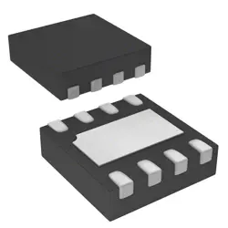
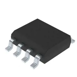
画像は参照用のみです。
BSC190N15NS3 G
MOSFETs N-Ch 150V 50A TDSON-8 OptiMOS 3
- メーカー
- Mfr。パート #BSC190N15NS3 G
- パッケージ
- データシート BSC190N15NS3 G DataSheet
- 在庫中25211
100% オリジナル &新しい
出荷の準備ができている24時間
365日の保証
RFQおよびもっと割引を得る
仕様
| Packaging | MouseReel |
| Standard Pack Qty | 5000 |
概要
Description
BSC190N15NS3 G is likely a course code for an introductory biology class. This course typically covers fundamental concepts in biology, including cellular structure, genetics, evolution, and ecology. It may also emphasize scientific inquiry, critical thinking, and laboratory skills. The "G" at the end of the code could indicate that it's a general education course, possibly aimed at non-majors or those seeking foundational knowledge in biological sciences.
Students can expect a mix of lectures, interactive discussions, and hands-on laboratory experiences, fostering an understanding of living organisms and their interactions with the environment. This course is essential for anyone interested in pursuing further studies in life sciences or related fields.
Students can expect a mix of lectures, interactive discussions, and hands-on laboratory experiences, fostering an understanding of living organisms and their interactions with the environment. This course is essential for anyone interested in pursuing further studies in life sciences or related fields.
Features
The BSC190N15NS3 G is a high-performance N-channel MOSFET designed for various power applications. Key features include:
1. Voltage Rating: It supports a maximum drain-to-source voltage (VDS) of 150V.
2. Current Rating: The continuous drain current (ID) is 190A, allowing for high current handling.
3. RDS(on): It offers a low on-resistance (RDS(on)) of approximately 0.015 ohms, enhancing efficiency and reducing power loss during operation.
4. Package Type: The device is typically available in a DPAK or similar package, facilitating easy mounting and thermal management.
5. Fast Switching Speed: It is designed for high-speed switching, making it suitable for applications like DC-DC converters, motor drives, and power inverters.
6. Thermal Performance: With a high maximum junction temperature rating, it provides reliable operation in demanding environments.
7. Gate Threshold Voltage: The gate threshold voltage (VGS(th)) ranges from 2 to 4V, enabling compatibility with low-voltage drive circuits.
Overall, the BSC190N15NS3 G is well-suited for high-efficiency power management solutions.
Package
The BSC190N15NS3 G is packaged in a TO-247 type housing. This package is designed for high-power applications, offering efficient thermal management and ease of mounting.
Pinout
The BSC190N15NS3 G is an N-channel MOSFET used in various power management applications. It features a total of 5 pins. The pin configuration and their functions are as follows:
1. Gate (G) - This pin is used to control the MOSFET's switching state. A voltage applied to the gate creates an electric field that allows current to flow between the drain and source.
2. Drain (D) - This is the terminal through which the main current flows out of the device when it is in the 'on' state.
3. Source (S) - This pin is connected to the ground or negative voltage in typical applications, allowing current to flow from the drain to the source when the MOSFET is activated.
4. Body Diode (internal) - The device has an internal body diode that provides a path for current in the reverse direction, useful for inductive load applications.
For specific applications, the datasheet should be consulted for detailed electrical characteristics and ratings.
Manufacturer
The BSC190N15NS3 G is manufactured by Infineon Technologies AG, a leading global semiconductor manufacturer based in Germany. Infineon specializes in designing and producing semiconductors for various applications, including automotive, industrial, and consumer electronics. The company is known for its innovations in power semiconductors, microcontrollers, and sensors, playing a crucial role in enabling energy efficiency and advanced technology solutions. Infineon focuses on developing products that support sustainable and efficient energy use, contributing to advancements in electrification and automation.
Application
The BSC190N15NS3 G is a N-channel MOSFET primarily used in power management applications. Its application areas include DC-DC converters, motor drives, and power supplies in automotive, industrial, and consumer electronics. It is suitable for high-efficiency switching applications due to its low on-resistance and fast switching capabilities.
Equivalent
The BSC190N15NS3 G chip is a N-channel MOSFET suitable for high-speed applications. Equivalent products include the Infineon BSC190N15NS4, STMicroelectronics STP190N15, and ON Semiconductor NTP190N15. Always verify specifications such as voltage, current ratings, and package types before substituting.
出荷
出荷方法私たち
DHL、FedEx、TNT、UPS、またはあなたの選択の他の運送業者を通じてグローバルな出荷サービスを提供します。
出荷料参照(DHL/FedEx):
DHL の: 配送費は25ドル〜45ドル(0.5kg)の範囲で、推定配送時間は2〜5営業日です。
フェデックス: 配送費は25ドル〜40ドル(0.5kg)の範囲で、推定配送時間は3〜7営業日。
UPS の: 配送費は25ドル〜45ドル(0.5kg)の範囲で、推定配送時間は3〜7営業日。
TNT社: 配送費は25ドル〜65ドル(0.5kg)の範囲で、推定配送時間は3〜7営業日。
EMS: 配送料金は30〜50ドル(0.5kg)の範囲で、推定配送時間は7〜15営業日です。
登録航空郵便: 配送費は2〜4ドル(0.1kg)で、推定配送時間は5〜20営業日です。
支払い
Payment Methods
支払い期間は100%前払いです。
現在、下記の支払い方法のみを受け入れています。:
1. ペイパル
2. クレジット・デビットカード
3. ワイヤー 転送
類似
-
![MX25V1635FZNQ03]() MX25V1635FZNQ03
Macronix
-
![MX25V16066M1I02]() MX25V16066M1I02
Macronix
-
![MX30LF2G28AD-TI]() MX30LF2G28AD-TI
Macronix
-
![MX25L8035EM2I-10G]() MX25L8035EM2I-10G
Macronix
-
![MX29GL512FHXFI-11G]() MX29GL512FHXFI-11..
Macronix
-
![MX25U3232FZBI02]() MX25U3232FZBI02
Macronix
-
![MX25L12833FZNI-10G]() MX25L12833FZNI-10..
Macronix
-
![MX25U25645GXDI00]() MX25U25645GXDI00
Macronix
-
![MX29F040CQI-70G]() MX29F040CQI-70G
Macronix
-
![MX25L4006EM2I-12G]() MX25L4006EM2I-12G
Macronix
-
![MX25R4035FM1IL0]() MX25R4035FM1IL0
Macronix
-
![MX25L6473FM2I-08G]() MX25L6473FM2I-08G
Macronix