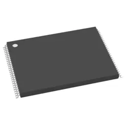
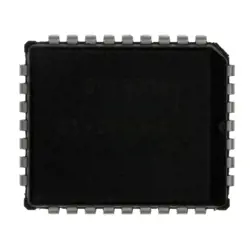
画像は参照用のみです。
AM29F400BB-70SE
- メーカー
- Mfr。パート #AM29F400BB-70SE
- パッケージ
- データシート
- 在庫中16096
100% オリジナル &新しい
出荷の準備ができている24時間
365日の保証
RFQおよびもっと割引を得る
仕様
| EU RoHS | Not Compliant |
| ECCN (US) | EAR99 |
| Part Status | Obsolete |
| HTS | 8542.32.00.71 |
| Automotive | No |
| PPAP | No |
| Cell Type | NOR |
| Chip Density (bit) | 4M |
| Architecture | Sectored |
| Boot Block | Yes |
| Number of Bits/Word (bit) | 8/16 |
| Number of Words | 512K/256K |
| Programmability | Yes |
| Timing Type | Asynchronous |
| Maximum Erase Time (S) | 8/Sector |
| Interface Type | Parallel |
| Minimum Operating Supply Voltage (V) | 4.5 |
| Typical Operating Supply Voltage (V) | 5 |
| Maximum Operating Supply Voltage (V) | 5.5 |
| Operating Current (mA) | 50 |
| Minimum Operating Temperature (°C) | -55 |
| Maximum Operating Temperature (°C) | 125 |
| Command Compatible | Yes |
| ECC Support | No |
| Support of Page Mode | No |
| Mounting | Surface Mount |
| Package Height | 2.3 |
| Package Width | 13.3 |
| Package Length | 28.2 |
| PCB changed | 44 |
| Standard Package Name | SO |
| Supplier Package | SO |
| Pin Count | 44 |
| Lead Shape | Gull-wing |
| Block Organization | Asymmetrical |
| Address Bus Width (bit) | 19/18 |
| Sector Size | 8Kbyte x 2|16Kbyte x 1|32Kbyte x 1|64Kbyte x 7 |
| Max. Access Time (ns) | 70 |
| Maximum Programming Time (ms) | 10800/Chip |
| Programming Voltage (V) | 4.5 to 5.5 |
| Program Current (mA) | 60 |
| Supplier Temperature Grade | Extended |
| SVHC | Yes |
| SVHC Exceeds Threshold | Yes |
| Location of Boot Block | Bottom |
| OE Access Time (ns) | 30 |
概要
Description
The AM29F400BB-70SE is a high-density, 4-megabit (512 K x 8) Flash memory device manufactured by Advanced Micro Devices (AMD). It utilizes a single 5V power supply and features a fast access time of 70 nanoseconds, making it suitable for a variety of applications, including embedded systems and firmware storage.
This EEPROM is designed for programming and erasing in sectors, allowing for more efficient use of memory. It supports both Byte and Word programming modes, and its typical architecture enables multiple read and write cycles. The chip incorporates a hardware write protection feature and can retain data for 20 years, ensuring reliability.
The AM29F400BB-70SE is typically used in applications requiring non-volatile memory, such as automotive, telecommunications, and consumer electronics, due to its durability and efficiency. Its compatibility with industry-standard interfaces facilitates integration into diverse systems.
Features
The AM29F400BB-70SE is a 4-Mbit (512 K x 8) Flash memory device, offering several key features:
1. Access Time: It has a maximum access time of 70 ns, ensuring quick data retrieval.
2. Voltage Range: Operates on a voltage range of 2.7V to 3.6V, suitable for low-power applications.
3. Interface: Utilizes a standard parallel interface for ease of integration.
4. Sector Architecture: Supports a sector architecture with 16 sectors of 32 KB each, enabling flexible programming and erasing.
5. Endurance: Offers a high endurance of 100,000 program/erase cycles per sector.
6. Data Retention: Ensures reliable data retention of 20 years at 125°C.
7. Programming Speed: Allows fast programming of 256 bytes in approximately 20 μs.
8. Single Supply Operation: Simplifies design with single-supply operation and low power consumption.
These features make the AM29F400BB-70SE suitable for various applications, including embedded systems and consumer electronics.
Package
The AM29F400BB-70SE is available in a 44-pin TSOP (Thin Small Outline Package) configuration. This package type is designed for surface-mount applications, offering a compact footprint for integrating the flash memory into electronic devices.
Pinout
The AM29F400BB-70SE is a 4 Megabit (512 K x 8) Flash memory device with a total of 40 pins. Its primary functions include:
1. Data Inputs/Outputs (D0-D7): Pins for data input and output.
2. Address Inputs (A0-A18): Pins used to select the address for read and write operations.
3. Chip Enable (CE): Activates the chip for operation.
4. Output Enable (OE): Controls the output of data from the memory.
5. Write Enable (WE): Enables the write operation to the memory.
6. Reset (RESET): Initializes the chip.
7. VCC: Power supply pin.
8. VSS: Ground pin.
9. Byte/Word Select (BLS): Used in multi-byte operations.
10. A19/A-1: Additional address pins for higher memory addressing.
The AM29F400BB-70SE is commonly used in embedded systems, providing non-volatile storage with fast access times.
Manufacturer
The AM29F400BB-70SE is manufactured by Advanced Micro Devices, Inc. (AMD), a prominent semiconductor company based in the United States. Founded in 1969, AMD is known for developing computer processors, graphics cards, and memory modules. The company has a strong focus on high-performance computing and has been a key player in the semiconductor industry, competing with other major firms like Intel and NVIDIA. AMD's product offerings include microprocessors for servers and personal computers, as well as embedded solutions. The AM29F400BB-70SE is a flash memory chip, part of AMD's legacy in providing memory solutions for embedded systems and other applications.
Application
The AM29F400BB-70SE is a 4-Mbit Flash memory device commonly used in embedded systems for applications such as:
1. Firmware storage in consumer electronics (e.g., TVs, appliances).
2. Automotive electronics for engine control units (ECUs).
3. Networking equipment like routers and switches.
4. Industrial control systems for programmable logic controllers (PLCs).
5. Medical devices for storing operational software and data.
Its non-volatile memory capability makes it ideal for applications requiring persistent data retention.
Equivalent
The AM29F400BB-70SE is a 4Mb (512KB x 8) Flash memory chip. Equivalent products include:
1. Intel 28F400 - A similar 4Mb Flash memory option.
2. Micron MT28F400 - Another compatible 4Mb Flash chip.
3. Spansion S29GL032 - While slightly larger, it's often used in similar applications.
Always verify pin compatibility and electrical characteristics when substituting components.
1. Intel 28F400 - A similar 4Mb Flash memory option.
2. Micron MT28F400 - Another compatible 4Mb Flash chip.
3. Spansion S29GL032 - While slightly larger, it's often used in similar applications.
Always verify pin compatibility and electrical characteristics when substituting components.
出荷
出荷方法私たち
DHL、FedEx、TNT、UPS、またはあなたの選択の他の運送業者を通じてグローバルな出荷サービスを提供します。
出荷料参照(DHL/FedEx):
DHL の: 配送費は25ドル〜45ドル(0.5kg)の範囲で、推定配送時間は2〜5営業日です。
フェデックス: 配送費は25ドル〜40ドル(0.5kg)の範囲で、推定配送時間は3〜7営業日。
UPS の: 配送費は25ドル〜45ドル(0.5kg)の範囲で、推定配送時間は3〜7営業日。
TNT社: 配送費は25ドル〜65ドル(0.5kg)の範囲で、推定配送時間は3〜7営業日。
EMS: 配送料金は30〜50ドル(0.5kg)の範囲で、推定配送時間は7〜15営業日です。
登録航空郵便: 配送費は2〜4ドル(0.1kg)で、推定配送時間は5〜20営業日です。
支払い
Payment Methods
支払い期間は100%前払いです。
現在、下記の支払い方法のみを受け入れています。:
1. ペイパル
2. クレジット・デビットカード
3. ワイヤー 転送
類似
-
![MX25R8035FM1IL0]() MX25R8035FM1IL0
Macronix
-
![MX25L3233FZBI-08Q]() MX25L3233FZBI-08Q
Macronix
-
![MX25L3233FM1I-08Q]() MX25L3233FM1I-08Q
Macronix
-
![MX25V1635FZNQ03]() MX25V1635FZNQ03
Macronix
-
![MX25V5126FM1I]() MX25V5126FM1I
Macronix
-
![MX25V16066M1I02]() MX25V16066M1I02
Macronix
-
![MX25R6435FBDIL0]() MX25R6435FBDIL0
Macronix
-
![MX25R1635FZUIH0]() MX25R1635FZUIH0
Macronix
-
![MX25U3232FZBI02]() MX25U3232FZBI02
Macronix
-
![MX25L12833FM2I-10G]() MX25L12833FM2I-10..
Macronix
-
![MX29LV160DTTI-70G]() MX29LV160DTTI-70G
Macronix
-
![MX29F040CQI-70G]() MX29F040CQI-70G
Macronix