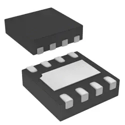
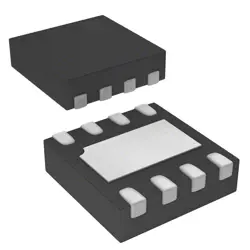
画像は参照用のみです。
ADS8341EB
IC ADC 16BIT SAR 16SSOP
- メーカー
- Mfr。パート #ADS8341EB
- パッケージ
- データシート ADS8341EB DataSheet
- 在庫中2676
100% オリジナル &新しい
出荷の準備ができている24時間
365日の保証
RFQおよびもっと割引を得る
仕様
| Part Status | Active |
| Number of Bits | 16 |
| Sampling Rate (Per Second) | 100k |
| Number of Inputs | 2, 4 |
| Input Type | Differential, Single Ended |
| Data Interface | SPI |
| Configuration | S/H-ADC |
| Ratio - S/H:ADC | 1:1 |
| Number of A/D Converters | 1 |
| Architecture | SAR |
| Reference Type | External |
| Voltage - Supply, Analog | 2.7V ~ 3.6V, 5V |
| Voltage - Supply, Digital | 2.7V ~ 3.6V, 5V |
| Operating Temperature | -40°C ~ 85°C |
| Package / Case | 16-SSOP (0.154", 3.90mm Width) |
| Supplier Device Package | 16-SSOP |
| Mounting Type | Surface Mount |
| Base Product Number | ADS8341 |
概要
Description
The ADS8341EB is an evaluation board designed for Texas Instruments' ADS8341, a 16-bit, successive approximation analog-to-digital converter (ADC). This ADC is optimized for applications requiring high precision and fast conversion rates, featuring a sampling rate of up to 100 kSPS.
The evaluation board provides an easy platform for testing and evaluating the performance of the ADS8341 in various configurations. It includes necessary support circuitry such as power supply circuits, reference voltage, and signal conditioning components, allowing users to interface the ADC with microcontrollers or other digital systems seamlessly.
Key features of the ADS8341EB include low power consumption, a parallel interface for quick data transfer, and an internal reference voltage option. This makes it suitable for applications in industrial automation, medical devices, and data acquisition systems. The board aids in understanding the device's functionalities and performance characteristics, facilitating rapid prototyping and design validation.
Features
The ADS8341EB is a high-performance, 16-bit analog-to-digital converter (ADC) designed for precision applications. Key features include:
1. Resolution: 16-bit conversion for high accuracy.
2. Sampling Rate: Up to 1.2 MSPS, allowing rapid data acquisition.
3. Input Voltage Range: Flexible input range with a unipolar configuration.
4. Low Power Consumption: Operates at a low supply current, suitable for battery-powered devices.
5. Integrated Reference: On-chip voltage reference simplifies design.
6. SPI Interface: Serial Peripheral Interface for easy communication with microcontrollers and digital systems.
7. Differential Inputs: Supports differential voltage measurements for enhanced noise immunity.
8. Wide Operating Temperature: Suitable for industrial applications with an extended temperature range.
9. Low Noise: High signal-to-noise ratio (SNR) for improved signal fidelity.
10. Programmable Gain Amplifier (PGA): Enhances signal processing capabilities.
These features make the ADS8341EB ideal for applications in industrial automation, data acquisition systems, and medical instrumentation.
Package
The ADS8341EB is packaged in a TQFP (Thin Quad Flat Package) with a 32-pin configuration. This package type provides a compact design suitable for surface mounting and efficient heat dissipation.
Pinout
The ADS8341EB is a 16-bit, low-power, analog-to-digital converter (ADC) with a pin count of 24 pins.
### Key Functions:
1. Power Supply Pins: VDD (Power supply for the ADC) and GND (Ground).
2. Analog Inputs: AIN0 to AIN3 (Analog input channels for the conversion).
3. Digital Interface:
- D0 to D15: Data output pins for the 16-bit digital representation of the analog input.
- SCLK: Serial clock for data clocking.
- DIN: Data input for configuration and control commands.
- DOUT: Data output for the converted digital signal.
4. Control Pins:
- CS: Chip select to enable the device.
- RD: Read control pin to initiate data transmission.
- REF: Reference voltage input for conversion accuracy.
5. Configuration Pins: Options for operating mode selections.
The ADS8341EB is used in applications requiring precise and efficient signal conversion, such as industrial automation and sensor interfacing.
Manufacturer
The ADS8341EB is manufactured by Texas Instruments (TI), a leading global semiconductor company. Texas Instruments specializes in the design and production of a wide range of semiconductor products, including analog and embedded processing devices. Founded in 1930, TI serves various industries such as automotive, industrial, communications, and consumer electronics. The company is known for its innovation in analog technologies and digital signal processing solutions.
Application
The ADS8341EB is a high-precision, 16-bit analog-to-digital converter (ADC) used in various application areas, including industrial automation, medical instrumentation, and data acquisition systems. It is suitable for precision measurements in process control, sensor interfacing, and handheld medical devices. Its features also make it ideal for battery-operated equipment, audio processing, and precision measurement in laboratory applications.
Equivalent
Equivalent products to the ADS8341EB chip include the following ADCs: ADS8342, ADS8343, and AD7791. These alternatives offer similar performance characteristics, including resolution and sampling rates, but may vary in features such as interface compatibility and supply voltage. Always consult datasheets for detailed specifications and compatibility for your specific application.
出荷
出荷方法私たち
DHL、FedEx、TNT、UPS、またはあなたの選択の他の運送業者を通じてグローバルな出荷サービスを提供します。
出荷料参照(DHL/FedEx):
DHL の: 配送費は25ドル〜45ドル(0.5kg)の範囲で、推定配送時間は2〜5営業日です。
フェデックス: 配送費は25ドル〜40ドル(0.5kg)の範囲で、推定配送時間は3〜7営業日。
UPS の: 配送費は25ドル〜45ドル(0.5kg)の範囲で、推定配送時間は3〜7営業日。
TNT社: 配送費は25ドル〜65ドル(0.5kg)の範囲で、推定配送時間は3〜7営業日。
EMS: 配送料金は30〜50ドル(0.5kg)の範囲で、推定配送時間は7〜15営業日です。
登録航空郵便: 配送費は2〜4ドル(0.1kg)で、推定配送時間は5〜20営業日です。
支払い
Payment Methods
支払い期間は100%前払いです。
現在、下記の支払い方法のみを受け入れています。:
1. ペイパル
2. クレジット・デビットカード
3. ワイヤー 転送
類似
-
![MX25R8035FM1IL0]() MX25R8035FM1IL0
Macronix
-
![MX25L3233FZBI-08Q]() MX25L3233FZBI-08Q
Macronix
-
![MX25L3233FM1I-08Q]() MX25L3233FM1I-08Q
Macronix
-
![MX25V1635FZNQ03]() MX25V1635FZNQ03
Macronix
-
![MX66U1G45GXDI00]() MX66U1G45GXDI00
Macronix
-
![MX25V2033FM1I]() MX25V2033FM1I
Macronix
-
![MX25V16066M1I02]() MX25V16066M1I02
Macronix
-
![MX25V16066M2I02]() MX25V16066M2I02
Macronix
-
![MX29GL512FHXFI-11G]() MX29GL512FHXFI-11..
Macronix
-
![MX25U25643GZNI00]() MX25U25643GZNI00
Macronix
-
![MX25R1635FZUIH0]() MX25R1635FZUIH0
Macronix
-
![MX25U3232FZBI02]() MX25U3232FZBI02
Macronix