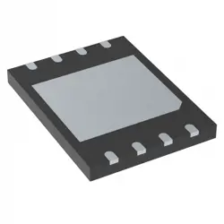
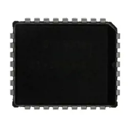
画像は参照用のみです。
ADN2850BCPZ250
DUAL 10-BIT SPI NVM DIGITAL RHEO
- メーカー
- Mfr。パート #ADN2850BCPZ250
- パッケージ LFCSP-16
- データシート ADN2850BCPZ250 DataSheet
- 在庫中2697
100% オリジナル &新しい
出荷の準備ができている24時間
365日の保証
RFQおよびもっと割引を得る
仕様
| Package | Bulk |
| ProductStatus | Active |
概要
Description
The ADN2850BCPZ250 is a high-performance, low-power clock and data recovery (CDR) chip designed for optical and wireless communications. It operates at data rates up to 250 Mbps and offers advanced features such as integrated equalization and phase-locked loop (PLL) technology, making it suitable for high-speed interfaces.
Key features include low jitter performance, which is crucial for maintaining signal integrity, and support for a variety of input signal types. The device is housed in a compact 16-lead LFCSP package, ensuring ease of integration into various systems.
Additionally, the ADN2850BCPZ250 provides a flexible architecture that can adapt to different applications, enhancing its versatility in telecommunications, data center equipment, and other high-speed communication systems. The combination of performance, power efficiency, and compact design makes it an ideal choice for modern digital communication solutions.
Key features include low jitter performance, which is crucial for maintaining signal integrity, and support for a variety of input signal types. The device is housed in a compact 16-lead LFCSP package, ensuring ease of integration into various systems.
Additionally, the ADN2850BCPZ250 provides a flexible architecture that can adapt to different applications, enhancing its versatility in telecommunications, data center equipment, and other high-speed communication systems. The combination of performance, power efficiency, and compact design makes it an ideal choice for modern digital communication solutions.
Features
The ADN2850BCPZ250 is a high-performance, low-power, integrated data and clock recovery device designed for high-speed optical communication applications. Key features include:
1. Data Rate Support: It supports data rates up to 2.5 Gbps.
2. Jitter Tolerance: Offers excellent jitter tolerance, making it suitable for various applications.
3. Integrated Functions: Combines a clock and data recovery (CDR) circuit with an integrated voltage-controlled oscillator (VCO).
4. Low Power Consumption: Designed for efficiency, it operates at low power levels, ideal for power-sensitive applications.
5. Flexible Input: Capable of accepting differential or single-ended input signals.
6. Programmable Features: Includes programmable settings for various operational parameters, allowing customization for specific applications.
7. Wide Operating Range: Operates over a wide temperature range, ensuring reliability in different environments.
This device is typically used in SONET/SDH, Ethernet, and other telecommunications systems.
1. Data Rate Support: It supports data rates up to 2.5 Gbps.
2. Jitter Tolerance: Offers excellent jitter tolerance, making it suitable for various applications.
3. Integrated Functions: Combines a clock and data recovery (CDR) circuit with an integrated voltage-controlled oscillator (VCO).
4. Low Power Consumption: Designed for efficiency, it operates at low power levels, ideal for power-sensitive applications.
5. Flexible Input: Capable of accepting differential or single-ended input signals.
6. Programmable Features: Includes programmable settings for various operational parameters, allowing customization for specific applications.
7. Wide Operating Range: Operates over a wide temperature range, ensuring reliability in different environments.
This device is typically used in SONET/SDH, Ethernet, and other telecommunications systems.
Package
The ADN2850BCPZ250 is packaged in a 16-lead LFCSP (Lead Frame Chip Scale Package) with a 3mm x 3mm footprint. This compact package type is designed for enhanced thermal performance and space efficiency in various applications.
Pinout
The ADN2850BCPZ250 is a high-performance, integrated clock data recovery (CDR) and retimer device designed for high-speed serial data applications. It features a 32-pin LFCSP (Lead Frame Chip Scale Package) form factor.
The primary functions of the ADN2850 include:
1. Clock Data Recovery: It extracts timing information from incoming serial data streams to regenerate the clock signal.
2. Retiming: It ensures minimal jitter on the output data, enhancing signal integrity for high-speed communication.
3. Support for Various Data Rates: It operates effectively at data rates ranging from 1.25 Gbps to 3.125 Gbps.
4. Integrated Equalization: It compensates for signal degradation over long transmission lines.
5. Low Power Consumption: Designed for efficiency, making it suitable for power-sensitive applications.
The pin configuration includes power supply pins, input/output data pins, control pins, and ground connections, facilitating its integration into various systems.
The primary functions of the ADN2850 include:
1. Clock Data Recovery: It extracts timing information from incoming serial data streams to regenerate the clock signal.
2. Retiming: It ensures minimal jitter on the output data, enhancing signal integrity for high-speed communication.
3. Support for Various Data Rates: It operates effectively at data rates ranging from 1.25 Gbps to 3.125 Gbps.
4. Integrated Equalization: It compensates for signal degradation over long transmission lines.
5. Low Power Consumption: Designed for efficiency, making it suitable for power-sensitive applications.
The pin configuration includes power supply pins, input/output data pins, control pins, and ground connections, facilitating its integration into various systems.
Manufacturer
The manufacturer of the ADN2850BCPZ250 is Analog Devices, Inc. Analog Devices is a prominent American semiconductor company that specializes in data conversion, signal processing, and amplification technologies. Founded in 1965, the company develops a wide range of high-performance analog, mixed-signal, and digital signal processing integrated circuits. Their products are widely used in various applications, including telecommunications, automotive, industrial automation, and consumer electronics, making them a key player in the electronic components industry.
Application
The ADN2850BCPZ250 is a high-speed, precision clock and data recovery (CDR) IC primarily used in telecommunications and data communication applications. Key areas include optical networks, high-speed Ethernet, digital video, and SDI (Serial Digital Interface) systems. It enhances signal integrity and reduces jitter, making it suitable for long-distance transmission in fiber-optic networks and high-frequency data links.
Equivalent
The ADN2850BCPZ250 is a low-power, high-speed laser diode driver. Equivalent products include the Texas Instruments THS3091, Maxim MAX3680, and the Analog Devices ADN2850. Always check specifications for compatibility, as performance and features may vary slightly between models.
出荷
出荷方法私たち
DHL、FedEx、TNT、UPS、またはあなたの選択の他の運送業者を通じてグローバルな出荷サービスを提供します。
出荷料参照(DHL/FedEx):
DHL の: 配送費は25ドル〜45ドル(0.5kg)の範囲で、推定配送時間は2〜5営業日です。
フェデックス: 配送費は25ドル〜40ドル(0.5kg)の範囲で、推定配送時間は3〜7営業日。
UPS の: 配送費は25ドル〜45ドル(0.5kg)の範囲で、推定配送時間は3〜7営業日。
TNT社: 配送費は25ドル〜65ドル(0.5kg)の範囲で、推定配送時間は3〜7営業日。
EMS: 配送料金は30〜50ドル(0.5kg)の範囲で、推定配送時間は7〜15営業日です。
登録航空郵便: 配送費は2〜4ドル(0.1kg)で、推定配送時間は5〜20営業日です。
支払い
Payment Methods
支払い期間は100%前払いです。
現在、下記の支払い方法のみを受け入れています。:
1. ペイパル
2. クレジット・デビットカード
3. ワイヤー 転送
類似
-
![MX25L3233FZBI-08Q]() MX25L3233FZBI-08Q
Macronix
-
![MX25L3233FM1I-08Q]() MX25L3233FM1I-08Q
Macronix
-
![MX29F400CBTI-70G]() MX29F400CBTI-70G
Macronix
-
![MX25R3235FZNIL0]() MX25R3235FZNIL0
Macronix
-
![MX30LF2G28AD-TI]() MX30LF2G28AD-TI
Macronix
-
![MX25L8035EM2I-10G]() MX25L8035EM2I-10G
Macronix
-
![MX25L25673GMI-10G]() MX25L25673GMI-10G
Macronix
-
![MX25U51279GXDR00]() MX25U51279GXDR00
Macronix
-
![MX25L6433FM2I-08G]() MX25L6433FM2I-08G
Macronix
-
![MX25L12833FZ2I-10G]() MX25L12833FZ2I-10..
Macronix
-
![MX25U25645GXDI00]() MX25U25645GXDI00
Macronix
-
![MX29F040CQI-70G]() MX29F040CQI-70G
Macronix