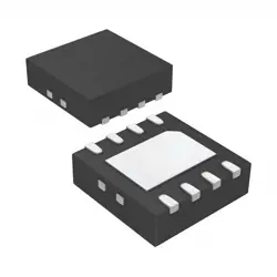
画像は参照用のみです。
ADN2813ACPZ
IC CLK DATA REC SDH 1.25GHZ
- メーカー
- Mfr。パート #ADN2813ACPZ
- パッケージ 32-WFQFN Exposed Pad, CSP
- データシート ADN2813ACPZ DataSheet
- 在庫中4241
100% オリジナル &新しい
出荷の準備ができている24時間
365日の保証
RFQおよびもっと割引を得る
仕様
| Package | Bulk,Tray |
| ProductStatus | Active |
| PLL | Yes |
| MainPurpose | SONET/SDH |
| Input | CML |
| Output | LVDS |
| NumberofCircuits | 1 |
| Ratio-Input:Output | 1:2 |
| Differential-Input:Output | Yes/Yes |
| Frequency-Max | 1.25GHz |
| Voltage-Supply | 3V ~ 3.6V |
| OperatingTemperature | -40°C ~ 85°C |
| MountingType | Surface Mount |
| Package/Case | 32-WFQFN Exposed Pad, CSP |
概要
Description
ADN2813ACPZ is a high-performance, low-power, integrated device designed for use in high-speed communication systems. It serves as a clock recovery and data retiming solution, particularly suited for applications in fiber optics and telecommunications. This device works with various data rates, typically up to 2.5 Gbps, and supports both 155 Mbps and 622 Mbps rates commonly used in SONET/SDH systems.
The ADN2813ACPZ features advanced jitter attenuation and processing capabilities, which enhance signal integrity and reduce timing errors in data streams. It includes features like programmable output levels and a wide supply voltage range, making it versatile for various system designs. The device comes in a compact 16-lead LFCSP package, facilitating easy integration into space-constrained environments.
Key applications include network switches, routers, and other telecommunication equipment that require reliable data transmission and clock recovery under challenging conditions. Overall, the ADN2813ACPZ is an essential component for engineers looking to improve the performance and reliability of high-speed digital communication systems.
The ADN2813ACPZ features advanced jitter attenuation and processing capabilities, which enhance signal integrity and reduce timing errors in data streams. It includes features like programmable output levels and a wide supply voltage range, making it versatile for various system designs. The device comes in a compact 16-lead LFCSP package, facilitating easy integration into space-constrained environments.
Key applications include network switches, routers, and other telecommunication equipment that require reliable data transmission and clock recovery under challenging conditions. Overall, the ADN2813ACPZ is an essential component for engineers looking to improve the performance and reliability of high-speed digital communication systems.
Features
The ADN2813ACPZ is a high-performance, low-power clock and data recovery (CDR) device designed for optical and digital communications. Key features include:
1. Data Rate Support: Operates at data rates between 155 Mbps to 2.5 Gbps, making it versatile for various applications.
2. Integrated PLL: Contains a phase-locked loop (PLL) for precise clock recovery from the input data stream.
3. Low Power Consumption: Designed for low power operation, which is ideal for energy-efficient applications.
4. Jitter Tolerance: Offers excellent jitter tolerance and output jitter performance, ensuring reliable data transmission.
5. Output Options: Provides differential and single-ended output options, facilitating integration into different system designs.
6. Automatic Equalization: Features automatic equalization for improved signal integrity over long connections.
7. Temperature Range: Operates over a wide temperature range, suitable for various environmental conditions.
8. Package: Available in a compact 32-lead LFCSP package, optimizing space in board designs.
These features make the ADN2813ACPZ suitable for applications in telecommunications, data centers, and high-speed networking.
1. Data Rate Support: Operates at data rates between 155 Mbps to 2.5 Gbps, making it versatile for various applications.
2. Integrated PLL: Contains a phase-locked loop (PLL) for precise clock recovery from the input data stream.
3. Low Power Consumption: Designed for low power operation, which is ideal for energy-efficient applications.
4. Jitter Tolerance: Offers excellent jitter tolerance and output jitter performance, ensuring reliable data transmission.
5. Output Options: Provides differential and single-ended output options, facilitating integration into different system designs.
6. Automatic Equalization: Features automatic equalization for improved signal integrity over long connections.
7. Temperature Range: Operates over a wide temperature range, suitable for various environmental conditions.
8. Package: Available in a compact 32-lead LFCSP package, optimizing space in board designs.
These features make the ADN2813ACPZ suitable for applications in telecommunications, data centers, and high-speed networking.
Package
The ADN2813ACPZ is packaged in a 16-lead LFCSP (Lead Frame Chip Scale Package) with a 3mm x 3mm size.
Pinout
The ADN2813ACPZ is a high-speed, low-power analog-to-digital converter (ADC) designed for use in various communication systems. It features a total of 28 pins.
Key functions of the pin configuration include:
1. Power Supply Pins: VDD and GND for power connections.
2. Signal Input Pins: For receiving differential input signals.
3. Reference Voltage Pins: To set the internal reference voltage.
4. Output Pins: For transmitting serialized data.
5. Control Pins: For configuration and control of various functionalities, including loop timing and fault indicators.
6. Clock Pins: For providing the necessary clock signals for operation.
The ADN2813 is commonly used in high-speed data links, fiber optics, and other communication applications, offering features like low jitter and high performance. For a precise application, refer to the datasheet for detailed pin functions and electrical characteristics.
Key functions of the pin configuration include:
1. Power Supply Pins: VDD and GND for power connections.
2. Signal Input Pins: For receiving differential input signals.
3. Reference Voltage Pins: To set the internal reference voltage.
4. Output Pins: For transmitting serialized data.
5. Control Pins: For configuration and control of various functionalities, including loop timing and fault indicators.
6. Clock Pins: For providing the necessary clock signals for operation.
The ADN2813 is commonly used in high-speed data links, fiber optics, and other communication applications, offering features like low jitter and high performance. For a precise application, refer to the datasheet for detailed pin functions and electrical characteristics.
Manufacturer
The ADN2813ACPZ is manufactured by Analog Devices, Inc. Analog Devices is a leading American multinational company that specializes in designing and manufacturing high-performance analog, mixed-signal, and digital signal processing (DSP) integrated circuits. Founded in 1965, the company serves various industries, including communications, automotive, industrial automation, and consumer electronics. Their products are widely used in applications that require precision and reliability, such as signal conditioning, data conversion, and advanced signal processing. Analog Devices is recognized for its innovation in analog technology and has a strong focus on research and development to meet the evolving needs of the electronics market.
Application
The ADN2813ACPZ is a high-speed, low-power data receiver primarily used in optical communication systems. Its application areas include fiber optic transceivers, high-speed Ethernet links, and telecommunications infrastructure. It is designed for use in data centers and network equipment, enabling reliable data transmission over long distances while minimizing signal degradation. Additionally, it can be utilized in various consumer electronics requiring high-speed data transfer.
Equivalent
Equivalent products to the ADN2813ACPZ chip include the following:
1. ADN2812 - A simpler version with fewer features.
2. LMH6626 - A high-speed comparator for similar applications.
3. MAX3675 - A different clock and data recovery solution.
Always check specific application requirements and datasheets for compatibility.
1. ADN2812 - A simpler version with fewer features.
2. LMH6626 - A high-speed comparator for similar applications.
3. MAX3675 - A different clock and data recovery solution.
Always check specific application requirements and datasheets for compatibility.
出荷
出荷方法私たち
DHL、FedEx、TNT、UPS、またはあなたの選択の他の運送業者を通じてグローバルな出荷サービスを提供します。
出荷料参照(DHL/FedEx):
DHL の: 配送費は25ドル〜45ドル(0.5kg)の範囲で、推定配送時間は2〜5営業日です。
フェデックス: 配送費は25ドル〜40ドル(0.5kg)の範囲で、推定配送時間は3〜7営業日。
UPS の: 配送費は25ドル〜45ドル(0.5kg)の範囲で、推定配送時間は3〜7営業日。
TNT社: 配送費は25ドル〜65ドル(0.5kg)の範囲で、推定配送時間は3〜7営業日。
EMS: 配送料金は30〜50ドル(0.5kg)の範囲で、推定配送時間は7〜15営業日です。
登録航空郵便: 配送費は2〜4ドル(0.1kg)で、推定配送時間は5〜20営業日です。
支払い
Payment Methods
支払い期間は100%前払いです。
現在、下記の支払い方法のみを受け入れています。:
1. ペイパル
2. クレジット・デビットカード
3. ワイヤー 転送
類似
-
![MX25L3233FZBI-08Q]() MX25L3233FZBI-08Q
Macronix
-
![MX25V1635FZNI]() MX25V1635FZNI
Macronix
-
![MX25V1635FZNQ03]() MX25V1635FZNQ03
Macronix
-
![MX25V4035FZUI]() MX25V4035FZUI
Macronix
-
![MX25V16066M2I02]() MX25V16066M2I02
Macronix
-
![MX25L8035EM2I-10G]() MX25L8035EM2I-10G
Macronix
-
![MX25R6435FBDIL0]() MX25R6435FBDIL0
Macronix
-
![MX29GL512FHXFI-11G]() MX29GL512FHXFI-11..
Macronix
-
![MX25L2006EM1I-12G]() MX25L2006EM1I-12G
Macronix
-
![MX25U6435FM2I-10G]() MX25U6435FM2I-10G
Macronix
-
![MX25U25645GXDI00]() MX25U25645GXDI00
Macronix
-
![MX25U51245GZ4I00]() MX25U51245GZ4I00
Macronix