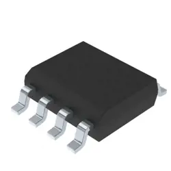
画像は参照用のみです。
ADF9010BCPZ
RFID RF IC
- メーカー
- Mfr。パート #ADF9010BCPZ
- パッケージ
- データシート ADF9010BCPZ DataSheet
- 在庫中5086
100% オリジナル &新しい
出荷の準備ができている24時間
365日の保証
RFQおよびもっと割引を得る
仕様
| Part Status | Active |
| Base Product Number | ADF9010 |
| RF Type | ISM |
| Frequency | 840MHz ~ 960MHz |
| Package | 48-WFQFN Exposed Pad, CSP |
| Supplier Device Package | 48-LFCSP (7x7) |
| Packaging | Tray |
概要
Description
The ADF9010BCPZ is a highly integrated RF transceiver designed for wireless communication applications. Manufactured by Analog Devices, it is part of their portfolio of RF components that are used in various communication systems. The chip typically features a wide range of functionalities, including frequency synthesis, modulation, and demodulation, making it suitable for complex wireless systems that require high performance and reliability.
The ADF9010BCPZ supports multiple frequency bands, providing flexibility for designers to use it in different applications such as cellular base stations, wireless infrastructure, and other broadband communication systems. It is built to deliver high linearity and low phase noise, which are critical for maintaining signal integrity in RF communications.
The package type, "BCPZ," indicates the specific packaging and pin configuration, which is essential for integration into circuit boards. The chip is engineered to be energy efficient, often incorporating power saving features to optimize performance in power-sensitive applications. Overall, the ADF9010BCPZ is a versatile component aimed at addressing the needs of modern RF communication systems.
Features
The ADF9010BCPZ is a mixed-signal integrated circuit designed for wireless communication applications. Key features include:
1. Frequency Range: Supports a wide frequency range, making it versatile for various RF applications.
2. Modulation Support: Capable of handling complex modulation schemes, suitable for modern communication standards.
3. Integrated VCO: Includes a Voltage-Controlled Oscillator, aiding in frequency synthesis without the need for external components.
4. PLL Functionality: Possesses a Phase-Locked Loop for stable frequency output, crucial for maintaining signal integrity.
5. Low Phase Noise: Delivers low phase noise performance, enhancing the signal quality in RF systems.
6. Power Efficiency: Designed to operate with low power consumption, beneficial for battery-powered devices.
7. Compact Package: The chip comes in a small footprint package (BCPZ), facilitating integration into space-constrained designs.
8. Digital Interfaces: Equipped with digital interfaces for easy control and configuration by the host processor.
These features make the ADF9010BCPZ suitable for applications in cellular infrastructure, point-to-point communication, and other RF communication systems where performance and integration are key.
Package
The ADF9010BCPZ is typically housed in a 32-lead LFCSP (Lead Frame Chip Scale Package). This type of package is compact and designed for advanced RF and microwave applications, offering efficient thermal performance and minimal parasitic inductance.
Pinout
The ADF9010BCPZ is a quad-band GSM/GPRS RF transceiver. It is designed for use in GSM/EDGE mobile communication applications. The device typically comes in a 76-lead Lead Frame Chip Scale Package (LFCSP), which is a plastic encapsulated package with a metal lead frame. However, the exact pin count and configuration can vary depending on the specific manufacturer and revision, so it is important to refer to the specific datasheet provided by the manufacturer for precise details.
The primary functions of the ADF9010BCPZ include RF signal processing for GSM and GPRS systems, encompassing tasks such as frequency conversion, modulation, and demodulation. It integrates multiple components necessary for RF communication, potentially including voltage-controlled oscillators (VCOs), phase-locked loops (PLLs), mixers, and filters. These components work together to handle the conversion between baseband and RF signals, enabling communication within mobile networks. For exact pin functions and detailed specifications, consulting the ADF9010BCPZ datasheet is recommended.
The primary functions of the ADF9010BCPZ include RF signal processing for GSM and GPRS systems, encompassing tasks such as frequency conversion, modulation, and demodulation. It integrates multiple components necessary for RF communication, potentially including voltage-controlled oscillators (VCOs), phase-locked loops (PLLs), mixers, and filters. These components work together to handle the conversion between baseband and RF signals, enabling communication within mobile networks. For exact pin functions and detailed specifications, consulting the ADF9010BCPZ datasheet is recommended.
Manufacturer
The ADF9010BCPZ is manufactured by Analog Devices, Inc. Analog Devices is a multinational semiconductor company specializing in the design, manufacture, and marketing of a broad portfolio of integrated circuits (ICs) used in analog and digital signal processing applications. The company provides solutions for various applications in industrial, automotive, consumer, and communication sectors, focusing on innovation in areas like data conversion, signal processing, power management, and radio frequency (RF) technology.
Application
The ADF9010BCPZ is typically used in wireless communication applications. It is well-suited for cellular infrastructure, wireless base stations, and RF communication systems. Its capabilities make it ideal for applications requiring frequency synthesis and modulation, such as GSM, CDMA, WCDMA, and LTE networks. Additionally, it can be used in satellite communications, point-to-point microwave links, and radar systems.
Equivalent
The ADF9010BCPZ is a dual-channel wideband synthesizer from Analog Devices. Equivalent products would typically include dual-channel synthesizers with similar frequency ranges and functionalities from other manufacturers. Potential equivalents could be products like Texas Instruments' LMX series or NXP's PLL with integrated VCOs, although exact matches may vary based on specific requirements such as frequency range, phase noise, and power consumption. Always check the latest datasheets and product specifications to ensure compatibility.
出荷
出荷方法私たち
DHL、FedEx、TNT、UPS、またはあなたの選択の他の運送業者を通じてグローバルな出荷サービスを提供します。
出荷料参照(DHL/FedEx):
DHL の: 配送費は25ドル〜45ドル(0.5kg)の範囲で、推定配送時間は2〜5営業日です。
フェデックス: 配送費は25ドル〜40ドル(0.5kg)の範囲で、推定配送時間は3〜7営業日。
UPS の: 配送費は25ドル〜45ドル(0.5kg)の範囲で、推定配送時間は3〜7営業日。
TNT社: 配送費は25ドル〜65ドル(0.5kg)の範囲で、推定配送時間は3〜7営業日。
EMS: 配送料金は30〜50ドル(0.5kg)の範囲で、推定配送時間は7〜15営業日です。
登録航空郵便: 配送費は2〜4ドル(0.1kg)で、推定配送時間は5〜20営業日です。
支払い
Payment Methods
支払い期間は100%前払いです。
現在、下記の支払い方法のみを受け入れています。:
1. ペイパル
2. クレジット・デビットカード
3. ワイヤー 転送
類似
-
![MX25L3233FM1I-08Q]() MX25L3233FM1I-08Q
Macronix
-
![MX25V1635FZNI]() MX25V1635FZNI
Macronix
-
![MX25V1635FZNQ03]() MX25V1635FZNQ03
Macronix
-
![MX66U1G45GXDI00]() MX66U1G45GXDI00
Macronix
-
![MX25V4035FZUI]() MX25V4035FZUI
Macronix
-
![MX25V2033FM1I]() MX25V2033FM1I
Macronix
-
![MX25L8035EM2I-10G]() MX25L8035EM2I-10G
Macronix
-
![MX25R6435FBDIL0]() MX25R6435FBDIL0
Macronix
-
![MX29GL512FHXFI-11G]() MX29GL512FHXFI-11..
Macronix
-
![MX25U51279GXDR00]() MX25U51279GXDR00
Macronix
-
![MX25V1635FM2I]() MX25V1635FM2I
Macronix
-
![MX25L6433FM2I-08G]() MX25L6433FM2I-08G
Macronix