
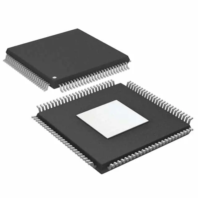
画像は参照用のみです。
A3P250-VQG100I
IC FPGA 68 I/O 100VQFP
- メーカー
- Mfr。パート #A3P250-VQG100I
- パッケージ TQFP-100
- データシート
- 在庫中3599
100% オリジナル &新しい
出荷の準備ができている24時間
365日の保証
RFQおよびもっと割引を得る
仕様
| Package | Tray |
| Series | ProASIC3 |
| ProductStatus | Active |
| TotalRAMBits | 36864 |
| NumberofI/O | 68 |
| NumberofGates | 250000 |
| Voltage-Supply | 1.425V ~ 1.575V |
| MountingType | Surface Mount |
| OperatingTemperature | -40°C ~ 100°C (TJ) |
| Package/Case | 100-TQFP |
概要
Description
The A3P250-VQG100I is a field-programmable gate array (FPGA) from Actel (now part of Microchip Technology). It belongs to the ProASIC3 family, known for its low power consumption and non-volatile architecture, making it suitable for applications where power efficiency is critical. The "250" in the name indicates that it has approximately 250,000 system gates, and "VQG100" refers to its package type, which is a 100-pin thin quad flat package (TQFP).
This FPGA supports various design features, including a range of I/O standards and clock management options, and it is programmable using hardware description languages like VHDL or Verilog. Ideal for embedded systems, automotive applications, and consumer electronics, the A3P250-VQG100I provides a balance of performance and power, along with the flexibility of reconfiguration, enabling designers to adapt their systems after deployment.
This FPGA supports various design features, including a range of I/O standards and clock management options, and it is programmable using hardware description languages like VHDL or Verilog. Ideal for embedded systems, automotive applications, and consumer electronics, the A3P250-VQG100I provides a balance of performance and power, along with the flexibility of reconfiguration, enabling designers to adapt their systems after deployment.
Features
The A3P250-VQG100I is a FPGA (Field-Programmable Gate Array) from Achronix's Speedster series. Key features include:
1. Logic Density: Approximately 250,000 usable logic gates, allowing for complex designs.
2. Speed: Optimized for high-speed applications with a maximum operating frequency of up to 500 MHz.
3. I/O Options: Supports multiple I/O standards, including LVTTL, LVCMOS, and others, with up to 100 pins for versatile connectivity.
4. Embedded Memory: Includes embedded SRAM blocks for efficient data storage and processing.
5. Flexibility: Fully programmable, allowing for custom logic design tailored to specific applications.
6. Power Efficiency: Designed for low power consumption, making it suitable for portable and battery-operated devices.
7. Development Tools: Compatible with Achronix's design tools and third-party software for easy design implementation.
8. Applications: Ideal for applications in communications, automotive, industrial control, and consumer electronics.
Overall, the A3P250-VQG100I combines performance, flexibility, and efficiency for a wide range of digital applications.
Package
The A3P250-VQG100I is packaged in a 100-pin VQFP (Very Thin Quad Flat Package) format. This package type is known for its compact size and is suitable for applications requiring high-density integration and performance.
Pinout
The A3P250-VQG100I is a FPGA (Field-Programmable Gate Array) from Actel (now part of Microchip Technology). It features a pin count of 100 pins in a VQFP (Very Thin Quad Flat Package) form factor.
The primary functions of the A3P250 include:
- Configurable Logic Blocks (CLBs): for implementing custom logic.
- I/O Blocks: which support various signaling standards for interfacing with other devices.
- Memory Blocks: including SRAM for data storage.
- Clock Management: capabilities for generating and distributing clock signals.
- Dedicated Configuration Pins: for programming and configuring the FPGA.
This device is utilized in applications such as digital signal processing, embedded systems, and custom hardware accelerators due to its flexibility and reprogrammability.
Manufacturer
The A3P250-VQG100I is manufactured by Achronix Semiconductor Corporation. Achronix is a technology company that specializes in high-performance field-programmable gate arrays (FPGAs) and embedded FPGA (eFPGA) solutions. Founded in 2004 and based in San Jose, California, Achronix focuses on delivering advanced semiconductor products for applications such as data centers, networking, and artificial intelligence. Their offerings are designed to provide high speed, flexibility, and efficiency, catering to the needs of modern computing architectures. Achronix has positioned itself as a key player in the FPGA market, competing with other established companies in the semiconductor industry.
Application
The A3P250-VQG100I is a field-programmable gate array (FPGA) primarily used in applications such as digital signal processing, embedded systems, industrial automation, telecommunications, and consumer electronics. Its low power consumption and flexibility make it suitable for real-time data processing, system on chip (SoC) designs, and custom hardware acceleration in various industries.
Equivalent
The A3P250-VQG100I chip, part of the Actel ProASIC3 family, has equivalent products such as the Lattice MachXO2-256, Xilinx Spartan-6 LX9, and Microsemi SmartFusion2 M2S050. These alternatives vary in features and specifications, so it's essential to consider the specific requirements of your application when selecting a substitute.
出荷
出荷方法私たち
DHL、FedEx、TNT、UPS、またはあなたの選択の他の運送業者を通じてグローバルな出荷サービスを提供します。
出荷料参照(DHL/FedEx):
DHL の: 配送費は25ドル〜45ドル(0.5kg)の範囲で、推定配送時間は2〜5営業日です。
フェデックス: 配送費は25ドル〜40ドル(0.5kg)の範囲で、推定配送時間は3〜7営業日。
UPS の: 配送費は25ドル〜45ドル(0.5kg)の範囲で、推定配送時間は3〜7営業日。
TNT社: 配送費は25ドル〜65ドル(0.5kg)の範囲で、推定配送時間は3〜7営業日。
EMS: 配送料金は30〜50ドル(0.5kg)の範囲で、推定配送時間は7〜15営業日です。
登録航空郵便: 配送費は2〜4ドル(0.1kg)で、推定配送時間は5〜20営業日です。
支払い
Payment Methods
支払い期間は100%前払いです。
現在、下記の支払い方法のみを受け入れています。:
1. ペイパル
2. クレジット・デビットカード
3. ワイヤー 転送
類似
-
![MX25V4035FZUI]() MX25V4035FZUI
Macronix
-
![MX25V16066M1I02]() MX25V16066M1I02
Macronix
-
![MX25R3235FZNIL0]() MX25R3235FZNIL0
Macronix
-
![MX30LF2G28AD-TI]() MX30LF2G28AD-TI
Macronix
-
![MX25L8035EM2I-10G]() MX25L8035EM2I-10G
Macronix
-
![MX29GL512FHXFI-11G]() MX29GL512FHXFI-11..
Macronix
-
![MX25R1635FZUIH0]() MX25R1635FZUIH0
Macronix
-
![MX25U3232FZBI02]() MX25U3232FZBI02
Macronix
-
![MX25L12833FM2I-10G]() MX25L12833FM2I-10..
Macronix
-
![MX25L12833FZ2I-10G]() MX25L12833FZ2I-10..
Macronix
-
![MX29F800CBTI-70G]() MX29F800CBTI-70G
Macronix
-
![MX29LV640ETTI-70G]() MX29LV640ETTI-70G
Macronix







