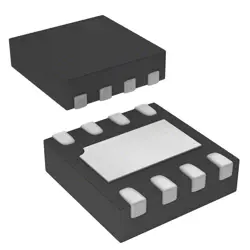
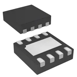
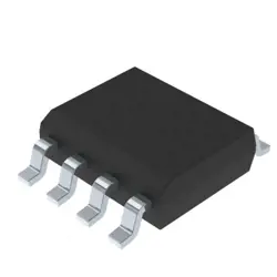
画像は参照用のみです。
74LVC2G04GV
Inverters
- メーカー
- Mfr。パート #74LVC2G04GV
- パッケージ
- データシート
- 在庫中12768
100% オリジナル &新しい
出荷の準備ができている24時間
365日の保証
RFQおよびもっと割引を得る
仕様
概要
Description
The 74LVC2G04GV is a dual buffer/driver IC from the 74LVC series, designed for low-voltage applications. It features two independent, non-inverting buffers, which can drive high-speed signals with low power consumption. Operating within a voltage range of 1.65V to 5.5V, this device is compatible with both TTL and CMOS logic levels, making it versatile for various circuit designs.
The 74LVC2G04GV offers high noise immunity and provides drive capability for a wide range of applications, including data processing, signal buffering, and level shifting. Its small package size (usually in a SOT-23 or similar) allows for space-efficient PCB designs.
Key specifications include high-speed operation (up to 5 GHz), low propagation delay, and the ability to drive up to 24 mA at output. This makes it suitable for applications in telecommunications, automotive, and consumer electronics. The device is also characterized by low static and dynamic power consumption, contributing to energy-efficient designs.
Features
The 74LVC2G04GV is a dual inverter buffer from the 74LVC family, featuring low-voltage CMOS technology. Key features include:
1. Dual Inverter Configuration: Contains two independent inverters, allowing for multiple signal inversion in one package.
2. Wide Voltage Range: Operates from 1.65V to 5.5V, making it suitable for various applications.
3. Low Power Consumption: Designed for low static and dynamic power usage, enhancing efficiency.
4. High-Speed Operation: Capable of switching at high frequencies, supporting fast signal processing.
5. TTL Compatibility: Compatible with TTL levels, facilitating integration with other logic families.
6. Wide Temperature Range: Operates effectively in temperatures from -40°C to +125°C.
7. Small Package: Available in a compact SOT23-5 package, ideal for space-constrained designs.
8. ESD Protection: Features built-in electrostatic discharge protection for enhanced reliability.
These attributes make the 74LVC2G04GV suitable for a variety of digital applications in consumer electronics, communications, and automotive systems.
Package
The 74LVC2G04GV is available in a small SOT-23 (SMT) package type. This compact package is suitable for surface mount applications, providing space-saving benefits in electronic circuit design.
Pinout
The 74LVC2G04GV is a dual inverter logic gate from the 74LVC series, featuring a total of 6 pins. It includes two independent inverter functions, which means it takes a single input and provides the inverted output.
### Pin Count and Functions:
- Pin 1 (A1): Input of the first inverter.
- Pin 2 (Y1): Output of the first inverter.
- Pin 3 (GND): Ground connection.
- Pin 4 (Y2): Output of the second inverter.
- Pin 5 (A2): Input of the second inverter.
- Pin 6 (VCC): Supply voltage connection.
### Key Features:
- Supply Voltage Range: 1.65V to 5.5V.
- Low power consumption.
- High-speed operation.
- Compatible with standard CMOS logic levels.
This device is often used in applications requiring signal inversion in digital logic circuits.
Manufacturer
The manufacturer of the 74LVC2G04GV is Nexperia. Nexperia is a global semiconductor company that specializes in discrete, logic, and MOSFET components. Initially part of Philips, Nexperia became an independent entity in 2017. The company focuses on high-quality semiconductor solutions for a variety of applications, including automotive, industrial, and consumer electronics. Nexperia is known for its commitment to reliability, efficiency, and innovation in its product offerings.
Application
The 74LVC2G04GV is a dual inverter (NOT gate) used in various applications including signal conditioning, level shifting, and logic manipulation in digital circuits. Its low power consumption and high-speed operation make it suitable for battery-operated devices, portable electronics, and communication systems. Additionally, it can be utilized in interfacing between different voltage levels in mixed-signal environments, enhancing signal integrity in embedded systems, and implementing simple logic functions in programmable logic devices.
Equivalent
The 74LVC2G04GV chip, a dual inverter buffer, has several equivalent products including:
1. 74LVC2G04
2. 74LVC1G04
3. 74HC14 (single inverter)
4. 74HCT14 (HCT version of 74HC14)
5. MC74LVC2G04 (Motorola variant)
Always check the datasheets for specific pinout, voltage, and temperature range compatibility.
1. 74LVC2G04
2. 74LVC1G04
3. 74HC14 (single inverter)
4. 74HCT14 (HCT version of 74HC14)
5. MC74LVC2G04 (Motorola variant)
Always check the datasheets for specific pinout, voltage, and temperature range compatibility.
出荷
出荷方法私たち
DHL、FedEx、TNT、UPS、またはあなたの選択の他の運送業者を通じてグローバルな出荷サービスを提供します。
出荷料参照(DHL/FedEx):
DHL の: 配送費は25ドル〜45ドル(0.5kg)の範囲で、推定配送時間は2〜5営業日です。
フェデックス: 配送費は25ドル〜40ドル(0.5kg)の範囲で、推定配送時間は3〜7営業日。
UPS の: 配送費は25ドル〜45ドル(0.5kg)の範囲で、推定配送時間は3〜7営業日。
TNT社: 配送費は25ドル〜65ドル(0.5kg)の範囲で、推定配送時間は3〜7営業日。
EMS: 配送料金は30〜50ドル(0.5kg)の範囲で、推定配送時間は7〜15営業日です。
登録航空郵便: 配送費は2〜4ドル(0.1kg)で、推定配送時間は5〜20営業日です。
支払い
Payment Methods
支払い期間は100%前払いです。
現在、下記の支払い方法のみを受け入れています。:
1. ペイパル
2. クレジット・デビットカード
3. ワイヤー 転送
類似
-
![MX29F400CBTI-70G]() MX29F400CBTI-70G
Macronix
-
![MX25R3235FZNIL0]() MX25R3235FZNIL0
Macronix
-
![MX25V16066M2I02]() MX25V16066M2I02
Macronix
-
![MX25R6435FBDIL0]() MX25R6435FBDIL0
Macronix
-
![MX25L25673GMI-08G]() MX25L25673GMI-08G
Macronix
-
![MX25L25673GMI-10G]() MX25L25673GMI-10G
Macronix
-
![MX25L2006EM1I-12G]() MX25L2006EM1I-12G
Macronix
-
![MX25R1635FZUIH0]() MX25R1635FZUIH0
Macronix
-
![MX25U3232FZBI02]() MX25U3232FZBI02
Macronix
-
![MX25L12835FZ2I-10G]() MX25L12835FZ2I-10..
Macronix
-
![MX25L4006EM2I-12G]() MX25L4006EM2I-12G
Macronix
-
![MX25V8035FM2I]() MX25V8035FM2I
Macronix