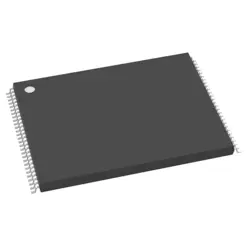
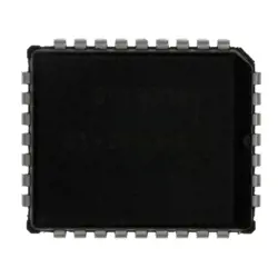
画像は参照用のみです。
74LVC244APW
Buffers & Line Drivers 3.3V OCTAL 3-S DRVER
- メーカー
- Mfr。パート #74LVC244APW
- パッケージ
- データシート
- 在庫中10338
100% オリジナル &新しい
出荷の準備ができている24時間
365日の保証
RFQおよびもっと割引を得る
仕様
| Standard Pack Qty | 75 |
概要
Description
The 74LVC244APW is an octal buffer/driver with 3-state outputs, designed for high-speed and low-power applications. It features a wide operating voltage range (1.65V to 5.5V), making it compatible with various digital logic families. The device has eight outputs that can drive capacitive loads, and it is ideal for data routing between different parts of a circuit.
The 74LVC244APW operates with low power consumption and offers fast switching times, making it suitable for high-performance applications. The 3-state outputs allow for multiple devices to share a common bus, enabling efficient data communication in systems like microcontrollers and FPGAs.
It comes in a 20-pin TSSOP package, providing a compact solution for space-constrained designs. The device also features CMOS technology, ensuring high noise immunity and low static power dissipation. Overall, the 74LVC244APW is a versatile component widely used in digital circuits requiring reliable buffering and driving capabilities.
Features
The 74LVC244APW is an octal buffer/driver designed for high-speed performance and low power consumption. Key features include:
1. Octal Configuration: Contains eight independent buffers/driver circuits.
2. Logic Levels: Compatible with both LVCMOS and TTL logic levels.
3. Wide Operating Voltage: Supports a supply voltage range from 1.8V to 5.5V.
4. High-Speed Operation: Offers fast propagation delays, making it suitable for high-speed applications.
5. Low Power Consumption: Maintains low static and dynamic power consumption, enhancing energy efficiency.
6. 3-State Outputs: Each output can be set to high, low, or high-impedance state, allowing for bus-oriented applications.
7. Pin and Function Compatible: With other 74xx series devices, enabling easy integration into existing designs.
8. ESD Protection: Enhanced electrostatic discharge protection for improved reliability.
This makes the 74LVC244APW ideal for use in data communication and memory interfacing applications.
Package
The 74LVC244APW is packaged in a TSSOP (Thin Shrink Small Outline Package) with 20 pins.
Pinout
The 74LVC244APW is an octal buffer/driver with 3-state outputs. It features a total of 20 pins. The key functions include:
- Data Inputs (A1 to A8): Pins 2-9 receive the input data.
- Output Enable (OE): Pin 1 controls the output state; when HIGH, the outputs are in a high-impedance state.
- Data Outputs (Y1 to Y8): Pins 11-18 provide the buffered output of the input data.
- VCC: Pin 20 is the power supply connection, typically +3.3V or +5V.
- GND: Pin 10 is the ground connection.
The device operates with low supply voltage and is compatible with both TTL and CMOS logic levels, making it suitable for various digital applications.
Manufacturer
The manufacturer of the 74LVC244APW is Nexperia. Nexperia is a global semiconductor company that specializes in the production of discrete, logic, and MOSFET components. It was formed from the divestiture of NXP Semiconductors' standard products division and operates independently, focusing on high-volume, high-quality semiconductor manufacturing. Nexperia provides a wide range of products used in various applications, including automotive, industrial, and consumer electronics.
Application
The 74LVC244APW is a low-voltage, high-speed hex buffer/driver with 3-state outputs. Its application areas include data buffering in digital circuits, signal amplification, driving LEDs, interfacing between different voltage levels, and increasing drive capability for bus systems. It is commonly used in communication devices, computing systems, and consumer electronics where reliable signal integrity and low power consumption are essential.
Equivalent
Equivalent products to the 74LVC244APW include the 74LVC244A, 74LVC244, and 74LVX244. Other compatible options may include the 74HC244 and 74HCT244, depending on specific application needs such as voltage levels and speed requirements. Always verify datasheets for pin compatibility and electrical characteristics.
出荷
出荷方法私たち
DHL、FedEx、TNT、UPS、またはあなたの選択の他の運送業者を通じてグローバルな出荷サービスを提供します。
出荷料参照(DHL/FedEx):
DHL の: 配送費は25ドル〜45ドル(0.5kg)の範囲で、推定配送時間は2〜5営業日です。
フェデックス: 配送費は25ドル〜40ドル(0.5kg)の範囲で、推定配送時間は3〜7営業日。
UPS の: 配送費は25ドル〜45ドル(0.5kg)の範囲で、推定配送時間は3〜7営業日。
TNT社: 配送費は25ドル〜65ドル(0.5kg)の範囲で、推定配送時間は3〜7営業日。
EMS: 配送料金は30〜50ドル(0.5kg)の範囲で、推定配送時間は7〜15営業日です。
登録航空郵便: 配送費は2〜4ドル(0.1kg)で、推定配送時間は5〜20営業日です。
支払い
Payment Methods
支払い期間は100%前払いです。
現在、下記の支払い方法のみを受け入れています。:
1. ペイパル
2. クレジット・デビットカード
3. ワイヤー 転送
類似
-
![MX25V1635FZNI]() MX25V1635FZNI
Macronix
-
![MX25R3235FZNIL0]() MX25R3235FZNIL0
Macronix
-
![MX30LF2G28AD-TI]() MX30LF2G28AD-TI
Macronix
-
![MX25L8035EM2I-10G]() MX25L8035EM2I-10G
Macronix
-
![MX25L25673GMI-08G]() MX25L25673GMI-08G
Macronix
-
![MX25U6435FM2I-10G]() MX25U6435FM2I-10G
Macronix
-
![MX25L12833FZ2I-10G]() MX25L12833FZ2I-10..
Macronix
-
![MX25U25645GXDI00]() MX25U25645GXDI00
Macronix
-
![MX25L12835FZ2I-10G]() MX25L12835FZ2I-10..
Macronix
-
![MX29LV160DTTI-70G]() MX29LV160DTTI-70G
Macronix
-
![MX29F040CQI-70G]() MX29F040CQI-70G
Macronix
-
![MX25L25645GXDI-08G]() MX25L25645GXDI-08..
Macronix