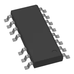
画像は参照用のみです。
74LV595PW
- メーカー
- Mfr。パート #74LV595PW
- パッケージ
- データシート
- 在庫中4320
100% オリジナル &新しい
出荷の準備ができている24時間
365日の保証
RFQおよびもっと割引を得る
仕様
| Shipping Restrictions | Mouser does not presently sell this product in your region. |
| Counting Sequence | Serial to Serial/Parallel |
| Number of Circuits | 1 Circuit |
| Number of Bits | 8 bit |
| Package / Case | TSSOP-16 |
| Logic Family | LV |
| Logic Type | CMOS |
| Number of Input Lines | 1 |
| Propagation Delay Time | 100 ns, 34 ns |
| Supply Voltage - Min | 1 V |
| Supply Voltage - Max | 3.6 V |
| Minimum Operating Temperature | - 40 C |
| Maximum Operating Temperature | + 125 C |
| Brand | Nexperia |
| Function | Shift Register |
| Mounting Style | SMD/SMT |
| Number of Output Lines | 9 Line |
| Product Type | Counter Shift Registers |
| Factory Pack Quantity:Factory Pack Quantity | 96 |
| Subcategory | Logic ICs |
| Width | 4.5 mm |
| Part # Aliases | 74LV595PW,112 |
| Unit Weight | 0.006102 oz |
| Operating Supply Voltage | 3.3 V |
| Height | 0.95 mm |
| Length | 5.1 mm |
| Supply Current - Max | 160 uA |
| Output Type | 3-State |
| Features | No Parallel Enable Input |
| Reset Type | Asynchronous |
| Triggering Type | Positive-Edge |
概要
Description
The 74LV595PW is a low-voltage 8-bit serial-in, serial or parallel-out shift register with a storage register and 3-state outputs. It operates from a supply voltage range of 1.0 V to 5.5 V, making it suitable for a variety of applications in low-power environments. This device is typically used in applications involving serial-to-parallel data conversion, allowing for efficient data communication and storage.
The 74LV595PW features an 8-bit shift register and an 8-bit storage register, which are both positive-edge-triggered. Data is shifted on the rising edge of the clock input, and it can be transferred to the output register either serially or in parallel. The outputs can be set to high-impedance, ensuring that multiple devices can share the same data lines.
This IC is often used in LED displays, data acquisition systems, and microcontroller interfacing to expand GPIO pins. It's encapsulated in a TSSOP (Thin Shrink Small Outline Package), which is compact and suitable for space-constrained applications. The device is part of the 74LV series, which is known for its low-voltage, low-power operation, and performance consistency across varying temperature ranges.
Features
The 74LV595PW is an 8-bit serial-in, parallel-out shift register with a storage register and 3-state outputs. It is part of the 74LV series of low-voltage CMOS devices. Key features include:
1. Low Voltage Operation: Operates at a voltage range of 1.0 V to 5.5 V, making it suitable for a wide variety of low-power applications.
2. High-Speed Operation: The device supports high-speed data transfer, facilitating rapid operation in digital circuits.
3. Serial Input and Parallel Output: Allows data to be input serially and output in parallel, useful for expanding I/O capabilities.
4. 3-State Outputs: The outputs can be set to a high-impedance state, allowing for easy bus interfacing and minimizing power consumption.
5. Latch Functionality: Data can be latched to maintain output even after the input data changes, providing stable performance.
6. Low Power Consumption: The device is designed to consume minimal power, ideal for battery-operated applications.
7. Wide Temperature Range: It operates effectively over a wide temperature range, ensuring reliability in various environments.
These features make the 74LV595PW versatile for use in digital circuits requiring efficient data handling and expansion.
Package
The 74LV595PW is a shift register IC from the 74LV series and comes in a TSSOP (Thin Shrink Small Outline Package) package type.
Pinout
The 74LV595PW is a 16-pin package IC, specifically a low-voltage CMOS device that functions as an 8-bit serial-in, serial or parallel-out shift register with an 8-bit storage register and tri-state outputs. It's commonly used for expanding the number of output pins in microcontroller applications.
Here is a brief overview of its pin functions:
1. Q0-Q7 (Pins 15, 1-7): Parallel output pins.
2. VCC (Pin 16): Supply voltage pin.
3. GND (Pin 8): Ground pin.
4. SER (Pin 14): Serial data input.
5. SRCLK (Pin 11): Shift register clock input, latching data into the shift register on the rising edge.
6. RCLK (Pin 12): Register clock input, transferring data from the shift register to the storage register on the rising edge.
7. /OE (Pin 13): Output enable, active low; controls the output buffers.
8. /SRCLR (Pin 10): Shift register clear, active low; clears the shift register when low.
The 74LV595PW is commonly used for cascading multiple shift registers to increase the number of I/O pins in digital systems.
Manufacturer
The 74LV595PW is manufactured by Nexperia, a company that specializes in the production of discrete and power semiconductor components. Nexperia was originally part of NXP Semiconductors but became an independent company in 2017. It focuses on manufacturing essential semiconductors that are used in various electronic devices, emphasizing efficiency and footprint reduction. Headquartered in Nijmegen, Netherlands, Nexperia operates globally and serves industries ranging from automotive to industrial and consumer electronics.
Application
The 74LV595PW is an 8-bit serial-in, parallel-out shift register with output latches. It is commonly used in applications requiring the expansion of output pins, such as LED displays, data buses, and digital output interfaces. Its ability to be daisy-chained makes it suitable for driving multiple outputs with limited microcontroller pins. Additionally, it's used in signal conversion and timing signal generation in various digital communication and control systems.
Equivalent
The 74LV595PW is a low-voltage 8-bit serial-in, parallel-out shift register with a storage register and 3-state outputs. Equivalent products include:
1. 74HC595N - NXP
2. SN74HC595 - Texas Instruments
3. MC74HC595ADTR2G - ON Semiconductor
4. CD74HC595M96 - Texas Instruments
5. TC74HC595AP - Toshiba
These components offer similar functionality with variations in electrical characteristics and packaging, so check compatibility with your specific application.
出荷
出荷方法私たち
DHL、FedEx、TNT、UPS、またはあなたの選択の他の運送業者を通じてグローバルな出荷サービスを提供します。
出荷料参照(DHL/FedEx):
DHL の: 配送費は25ドル〜45ドル(0.5kg)の範囲で、推定配送時間は2〜5営業日です。
フェデックス: 配送費は25ドル〜40ドル(0.5kg)の範囲で、推定配送時間は3〜7営業日。
UPS の: 配送費は25ドル〜45ドル(0.5kg)の範囲で、推定配送時間は3〜7営業日。
TNT社: 配送費は25ドル〜65ドル(0.5kg)の範囲で、推定配送時間は3〜7営業日。
EMS: 配送料金は30〜50ドル(0.5kg)の範囲で、推定配送時間は7〜15営業日です。
登録航空郵便: 配送費は2〜4ドル(0.1kg)で、推定配送時間は5〜20営業日です。
支払い
Payment Methods
支払い期間は100%前払いです。
現在、下記の支払い方法のみを受け入れています。:
1. ペイパル
2. クレジット・デビットカード
3. ワイヤー 転送
類似
-
![MX25R8035FM1IL0]() MX25R8035FM1IL0
Macronix
-
![MX25L3233FZBI-08Q]() MX25L3233FZBI-08Q
Macronix
-
![MX30LF2G28AD-TI]() MX30LF2G28AD-TI
Macronix
-
![MX25R6435FBDIL0]() MX25R6435FBDIL0
Macronix
-
![MX25L25673GMI-10G]() MX25L25673GMI-10G
Macronix
-
![MX25U25643GZNI00]() MX25U25643GZNI00
Macronix
-
![MX25R1635FZUIH0]() MX25R1635FZUIH0
Macronix
-
![MX25L12833FZ2I-10G]() MX25L12833FZ2I-10..
Macronix
-
![MX29F040CQI-70G]() MX29F040CQI-70G
Macronix
-
![MX25L25645GXDI-08G]() MX25L25645GXDI-08..
Macronix
-
![MX29LV640ETTI-70G]() MX29LV640ETTI-70G
Macronix
-
![MX25L25735FMI-10G]() MX25L25735FMI-10G
Macronix