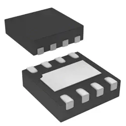
画像は参照用のみです。
74LCX125MX
BUS DRIVER, LVC/LCX/Z SERIES, 4-
- メーカー
- Mfr。パート #74LCX125MX
- パッケージ
- データシート 74LCX125MX DataSheet
- 在庫中2132
100% オリジナル &新しい
出荷の準備ができている24時間
365日の保証
RFQおよびもっと割引を得る
仕様
| Supplier | Rochester Electronics, LLC |
| Package | Bulk |
| ProductStatus | Active |
概要
Description
74LCX125MX is a quad buffer/driver with tri-state (3-state) outputs built on a low-power CMOS LCX process. It contains four independent noninverting buffer sections; each has its own active-low output-enable (OE). When OE is low, the corresponding input passes to the output; when OE is high, the output is high-impedance. This allows you to buffer signals, isolate devices on a shared bus, or perform level shifting between domains.
Key points:
- Four buffers with separate OE inputs
- Noninverting data path
- Outputs go hi-Z when enabled (OE high)
- Suitable for buffering/isolating digital signals and bus sharing
- Low-power LCX family device; CMOS/TTL-compatible inputs
Typical uses: expanding fan-out from a microcontroller, buffering data/address buses, or acting as a controllable buffer between subsystems.
For exact electrical specs (voltage range, drive, timing, and package details), refer to the specific 74LCX125MX datasheet.
Features
Key features of 74LCX125MX:
- Quad noninverting buffers with 3-state outputs (four independent buffers)
- Each buffer has its own output-enable input (tri‑state control)
- Outputs go high impedance when disabled, suitable for bus interfacing
- CMOS low-power LCX technology with relatively wide Vcc range
- Operates typically at 2.7–3.6 V (3.3 V systems common)
- TTL/CMOS input compatibility, robust ESD protection
- Fast switching suitable for medium-speed logic applications
- 14-pin package variant (MX) available (e.g., SOIC-14/DIP-14 formats)
Applications include bus interfacing, level shifting between parts, and any circuit requiring four independent buffers with tri-state outputs.
Package
MX indicates a molded small-outline package. The 74LCX125MX is a 14-pin plastic Small Outline package (SOIC-14).
Pinout
Pin count: 14 pins (14‑pin package).
Function: Quad buffer/line driver with 3‑state outputs. It contains four independent non‑inverting buffers (A1→Y1, A2→Y2, A3→Y3, A4→Y4) each with its own active‑low output enable (OE1–OE4). When OE is low, the input is passed to the output; when OE is high, the corresponding output is high impedance.
Function: Quad buffer/line driver with 3‑state outputs. It contains four independent non‑inverting buffers (A1→Y1, A2→Y2, A3→Y3, A4→Y4) each with its own active‑low output enable (OE1–OE4). When OE is low, the input is passed to the output; when OE is high, the corresponding output is high impedance.
Manufacturer
Manufacturer: Nexperia (a Dutch semiconductor company, spun off from NXP/Philips).
What kind of company: A global semiconductor company that designs and manufactures discrete components and logic integrated circuits used in electronics.
What kind of company: A global semiconductor company that designs and manufactures discrete components and logic integrated circuits used in electronics.
Application
74LCX125MX is a quad buffer/line driver with 3-state outputs. Common applications:
- Buffering and isolating data/address bus signals in microprocessor/microcontroller systems
- Level-shifting between different logic voltages (e.g., 5V to 3.3V)
- Driving multiple loads or long lines to reduce CPU load
- Enabling/disabling data paths with OE for tri-state bus sharing and multiplexing
- Backplane/general bus interface signaling and signal conditioning
Equivalent
74LCX125MX is a 4‑bit quad buffer/line driver with 3-state outputs. Equivalents (quad 3-state buffers):
- TI: SN74LCX125, SN74LVC125A (MX is just the package)
- ON Semiconductor: MC74LCX125A, MC74LCX125MX
- NXP/Nexperia: 74LCX125 (and 74LVC125A variants)
- STMicroelectronics: 74LVC125A
Note: all are functionally equivalent; choose based on voltage/pin/package needs.
- TI: SN74LCX125, SN74LVC125A (MX is just the package)
- ON Semiconductor: MC74LCX125A, MC74LCX125MX
- NXP/Nexperia: 74LCX125 (and 74LVC125A variants)
- STMicroelectronics: 74LVC125A
Note: all are functionally equivalent; choose based on voltage/pin/package needs.
出荷
出荷方法私たち
DHL、FedEx、TNT、UPS、またはあなたの選択の他の運送業者を通じてグローバルな出荷サービスを提供します。
出荷料参照(DHL/FedEx):
DHL の: 配送費は25ドル〜45ドル(0.5kg)の範囲で、推定配送時間は2〜5営業日です。
フェデックス: 配送費は25ドル〜40ドル(0.5kg)の範囲で、推定配送時間は3〜7営業日。
UPS の: 配送費は25ドル〜45ドル(0.5kg)の範囲で、推定配送時間は3〜7営業日。
TNT社: 配送費は25ドル〜65ドル(0.5kg)の範囲で、推定配送時間は3〜7営業日。
EMS: 配送料金は30〜50ドル(0.5kg)の範囲で、推定配送時間は7〜15営業日です。
登録航空郵便: 配送費は2〜4ドル(0.1kg)で、推定配送時間は5〜20営業日です。
支払い
Payment Methods
支払い期間は100%前払いです。
現在、下記の支払い方法のみを受け入れています。:
1. ペイパル
2. クレジット・デビットカード
3. ワイヤー 転送
類似
-
![MX25R8035FM1IL0]() MX25R8035FM1IL0
Macronix
-
![MX25V1635FZNI]() MX25V1635FZNI
Macronix
-
![MX25V1635FZNQ03]() MX25V1635FZNQ03
Macronix
-
![MX66U1G45GXDI00]() MX66U1G45GXDI00
Macronix
-
![MX25V4035FZUI]() MX25V4035FZUI
Macronix
-
![MX25V16066M1I02]() MX25V16066M1I02
Macronix
-
![MX25V16066M2I02]() MX25V16066M2I02
Macronix
-
![MX25L25673GMI-08G]() MX25L25673GMI-08G
Macronix
-
![MX25U51279GXDR00]() MX25U51279GXDR00
Macronix
-
![MX25R1635FZUIH0]() MX25R1635FZUIH0
Macronix
-
![MX25L6433FM2I-08G]() MX25L6433FM2I-08G
Macronix
-
![MX25U6435FM2I-10G]() MX25U6435FM2I-10G
Macronix