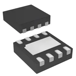
画像は参照用のみです。
74AVC9112GTX
74AVC9112GT/SOT833/XSON8
- メーカー
- Mfr。パート #74AVC9112GTX
- パッケージ 8-XFDFN
- データシート
- 在庫中3365
100% オリジナル &新しい
出荷の準備ができている24時間
365日の保証
RFQおよびもっと割引を得る
仕様
| Supplier | Nexperia USA Inc. |
| Package | Tape & Reel (TR),Cut Tape (CT) |
| Series | 74AVC |
| ProductStatus | Active |
| Type | Fanout Buffer (Distribution) |
| NumberofCircuits | 1 |
| Ratio-Input:Output | 1:4 |
| Differential-Input:Output | No/No |
| Input | Clock |
| Output | Clock |
| Voltage-Supply | 0.8V ~ 3.6V |
| OperatingTemperature | -40°C ~ 125°C (TA) |
| MountingType | Surface Mount |
| Package/Case | 8-XFDFN |
概要
Description
74AVC9112GTX is a 12-channel high-speed buffer/driver in the 74AVC logic family (NXP/Nexperia). It provides 12 non‑inverting buffer outputs with a common output enable (high‑Z when disabled). It's designed for fast data buffering and driving multiple loads, often used to isolate or level‑shift signals between devices or voltage domains. Features typically include a wide supply range, low static/dynamic power, and Ioff for partial-power-down protection. The GTX suffix relates to a specific packaging/assembly option (check the datasheet for exact package, pinout, and ordering info). For precise specs (drive strength, propagation delay, voltage ranges, and timing), consult the latest datasheet.
Features
Here are concise, typical features for the 74AVC9112GTX (AVC family) device:
- 12-bit bidirectional bus interface with tri-state outputs (OE control)
- Supply voltage: 2.7 V to 5.5 V (interfacing multiple logic levels)
- High-speed CMOS performance suitable for fast bus operations
- Ioff/partial-power-down protection (no back-powering when Vcc = 0)
- TTL/CMOS-compatible input thresholds
- Low static and dynamic power; energy-efficient operation
- ESD protection on all inputs/outputs
- RoHS-compliant, lead-free GTX packaging (tape-and-reel)
Common use cases: buffering/interfacing between buses, level shifting between voltage domains, and interconnect buffering in high-speed digital systems.
Note: exact electrical specs (propagation delay, drive strength, current limits) are device-specific—consult the official datasheet for precise numbers.
Package
The 74AVC9112GTX is supplied in a 14‑pin TSSOP (thin‑shrink small‑outline) package, lead‑free and tape‑and‑reel. Please verify exact dimensions and markings in the manufacturer's datasheet.
Manufacturer
Manufacturer: Nexperia.
What kind of company: Nexperia is a global semiconductor manufacturer (originally spun out of NXP) that specializes in standard logic ICs, discrete components and MOSFETs for automotive, industrial and consumer electronics applications.
What kind of company: Nexperia is a global semiconductor manufacturer (originally spun out of NXP) that specializes in standard logic ICs, discrete components and MOSFETs for automotive, industrial and consumer electronics applications.
Application
- Octal buffer/driver with 3-state outputs for high-speed data/address bus buffering between CPUs, FPGAs, and ASICs
- Fan-out and level shifting for 3.3V/5V interfaces
- Bus isolation and I/O expansion for microcontrollers and memory interfaces
- Backplane/video/data bus driving in consumer and industrial electronics
- Automotive/industrial digital I/O interfacing with fast edges and low power
- Fan-out and level shifting for 3.3V/5V interfaces
- Bus isolation and I/O expansion for microcontrollers and memory interfaces
- Backplane/video/data bus driving in consumer and industrial electronics
- Automotive/industrial digital I/O interfacing with fast edges and low power
Equivalent
I don’t have live web access to confirm exact cross‑references. To give correct equivalents I need the 74AVC9112GTX datasheet or its function (voltage translator/buffer, bit‑width, direction, package). Alternatively, you can find equivalents by matching family (74AVC), VCC range, I/O type, pinout and package using vendor cross‑reference tools (TI, Nexperia, ON Semiconductor, Octopart). Provide the datasheet or allow me to look it up and I’ll list direct drop‑in replacements.
出荷
出荷方法私たち
DHL、FedEx、TNT、UPS、またはあなたの選択の他の運送業者を通じてグローバルな出荷サービスを提供します。
出荷料参照(DHL/FedEx):
DHL の: 配送費は25ドル〜45ドル(0.5kg)の範囲で、推定配送時間は2〜5営業日です。
フェデックス: 配送費は25ドル〜40ドル(0.5kg)の範囲で、推定配送時間は3〜7営業日。
UPS の: 配送費は25ドル〜45ドル(0.5kg)の範囲で、推定配送時間は3〜7営業日。
TNT社: 配送費は25ドル〜65ドル(0.5kg)の範囲で、推定配送時間は3〜7営業日。
EMS: 配送料金は30〜50ドル(0.5kg)の範囲で、推定配送時間は7〜15営業日です。
登録航空郵便: 配送費は2〜4ドル(0.1kg)で、推定配送時間は5〜20営業日です。
支払い
Payment Methods
支払い期間は100%前払いです。
現在、下記の支払い方法のみを受け入れています。:
1. ペイパル
2. クレジット・デビットカード
3. ワイヤー 転送
類似
-
![MX25V1635FZNI]() MX25V1635FZNI
Macronix
-
![MX29F400CBTI-70G]() MX29F400CBTI-70G
Macronix
-
![MX66U1G45GXDI00]() MX66U1G45GXDI00
Macronix
-
![MX25R3235FZNIL0]() MX25R3235FZNIL0
Macronix
-
![MX25V16066M2I02]() MX25V16066M2I02
Macronix
-
![MX25L8035EM2I-10G]() MX25L8035EM2I-10G
Macronix
-
![MX25L2006EM1I-12G]() MX25L2006EM1I-12G
Macronix
-
![MX25U3232FZBI02]() MX25U3232FZBI02
Macronix
-
![MX25U6435FM2I-10G]() MX25U6435FM2I-10G
Macronix
-
![MX25L12835FZ2I-10G]() MX25L12835FZ2I-10..
Macronix
-
![MX29LV160DTTI-70G]() MX29LV160DTTI-70G
Macronix
-
![MX29F040CQI-70G]() MX29F040CQI-70G
Macronix