
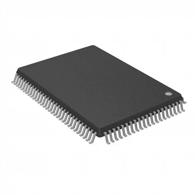
画像は参照用のみです。
70V27L20PFGI
IC SRAM 512KBIT PARALLEL 100TQFP
- メーカー
- Mfr。パート #70V27L20PFGI
- パッケージ 100-LQFP
- データシート
- 在庫中7391
100% オリジナル &新しい
出荷の準備ができている24時間
365日の保証
RFQおよびもっと割引を得る
仕様
| Package | Tray |
| ProductStatus | Active |
| MemoryType | Volatile |
| MemoryFormat | SRAM |
| Technology | SRAM - Dual Port, Asynchronous |
| MemorySize | 512Kb (32K x 16) |
| MemoryInterface | Parallel |
| WriteCycleTime-WordPage | 20ns |
| AccessTime | 20 ns |
| Voltage-Supply | 3V ~ 3.6V |
| OperatingTemperature | -40°C ~ 85°C (TA) |
| MountingType | Surface Mount |
| Package/Case | 100-LQFP |
概要
Description
The 70V27L20PFGI is a specific type of FPGA (Field-Programmable Gate Array) from the Intel (formerly Altera) 70V family. It features a combination of logic elements, high-speed I/Os, and flexible routing architecture, making it suitable for various applications such as digital signal processing, embedded systems, and custom logic design.
Key specifications include:
- Logic Elements: A large number of configurable logic blocks that can be programmed to perform a variety of tasks.
- I/O Capabilities: Supports multiple I/O standards for interfacing with other components and systems.
- Performance: High-speed operation, allowing for efficient data processing and real-time applications.
- Programmability: Can be reconfigured as needed, enabling rapid prototyping and design iterations.
This FPGA is ideal for engineers and developers looking to implement complex digital circuits without the need for custom silicon, providing flexibility and scalability in hardware design.
Key specifications include:
- Logic Elements: A large number of configurable logic blocks that can be programmed to perform a variety of tasks.
- I/O Capabilities: Supports multiple I/O standards for interfacing with other components and systems.
- Performance: High-speed operation, allowing for efficient data processing and real-time applications.
- Programmability: Can be reconfigured as needed, enabling rapid prototyping and design iterations.
This FPGA is ideal for engineers and developers looking to implement complex digital circuits without the need for custom silicon, providing flexibility and scalability in hardware design.
Features
The 70V27L20PFGI is a high-performance, low-power embedded processor designed for various applications, particularly in industrial and automotive sectors. Key features include:
1. Architecture: It utilizes a 32-bit architecture, providing efficient processing capabilities.
2. Speed: Offers clock speeds up to 200 MHz, facilitating rapid data processing.
3. Memory Support: Supports up to 2MB of flash memory and 512KB of SRAM, allowing for robust application performance.
4. I/O Interfaces: Equipped with multiple I/O interfaces including UART, SPI, and I2C, enabling versatile connectivity options.
5. Power Efficiency: Designed for low power consumption, making it suitable for battery-operated devices.
6. Integrated Peripherals: Includes integrated ADCs and PWM modules for enhanced functionality in control applications.
7. Operating Temperature Range: Supports a wide operating temperature range, ensuring reliability in harsh environments.
8. Development Tools: Compatible with various development tools and IDEs for ease of programming and deployment.
Overall, the 70V27L20PFGI is ideal for applications requiring efficient processing, flexibility, and reliability.
1. Architecture: It utilizes a 32-bit architecture, providing efficient processing capabilities.
2. Speed: Offers clock speeds up to 200 MHz, facilitating rapid data processing.
3. Memory Support: Supports up to 2MB of flash memory and 512KB of SRAM, allowing for robust application performance.
4. I/O Interfaces: Equipped with multiple I/O interfaces including UART, SPI, and I2C, enabling versatile connectivity options.
5. Power Efficiency: Designed for low power consumption, making it suitable for battery-operated devices.
6. Integrated Peripherals: Includes integrated ADCs and PWM modules for enhanced functionality in control applications.
7. Operating Temperature Range: Supports a wide operating temperature range, ensuring reliability in harsh environments.
8. Development Tools: Compatible with various development tools and IDEs for ease of programming and deployment.
Overall, the 70V27L20PFGI is ideal for applications requiring efficient processing, flexibility, and reliability.
Package
The package type of the 70V27L20PFGI is typically a TQFP (Thin Quad Flat Package) or similar surface-mount package, designed for compact installation on circuit boards. Please verify with specific manufacturer data sheets for precise details.
Pinout
The 70V27L20PFGI is a 32-pin programmable logic device from Lattice Semiconductor. It belongs to the ISP (In-System Programmable) family and is based on the architecture of a 256 x 8-bit EEPROM.
Pin Count: 32 pins
Function: The 70V27L20PFGI primarily serves as a programmable logic device, allowing users to implement custom logic functions, state machines, and various digital circuits. It features a 20 ns access time and provides the capability for in-system programming, making it versatile for applications in telecommunications, network equipment, and consumer electronics. The device can be configured to perform combinatorial logic and sequential logic functions, and its features include multiple input/output configurations, providing flexibility for different design requirements.
Pin Count: 32 pins
Function: The 70V27L20PFGI primarily serves as a programmable logic device, allowing users to implement custom logic functions, state machines, and various digital circuits. It features a 20 ns access time and provides the capability for in-system programming, making it versatile for applications in telecommunications, network equipment, and consumer electronics. The device can be configured to perform combinatorial logic and sequential logic functions, and its features include multiple input/output configurations, providing flexibility for different design requirements.
Manufacturer
The manufacturer of the 70V27L20PFGI is NXP Semiconductors, a global semiconductor company. NXP specializes in delivering high-performance mixed-signal and standard product solutions for a wide range of automotive, industrial, and consumer applications. The company is known for its focus on innovation in areas such as automotive safety, secure connectivity, and Internet of Things (IoT) technologies. NXP was formed in 2006 when Philips spun off its semiconductor division and has since grown through various acquisitions, enhancing its portfolio and market presence.
Application
The 70V27L20PFGI is a low-power, high-performance 32-bit microprocessor primarily used in embedded systems. Its application areas include industrial automation, automotive control systems, consumer electronics, IoT devices, telecommunications, and robotics. It is suitable for tasks requiring efficient processing and low power consumption, such as data acquisition, sensor management, and real-time control applications.
Equivalent
The 70V27L20PFGI is a CMOS SRAM, and its equivalents include the 70V27L20PFG, 70V27L20PGI, and other similar SRAM models like the 70V27L20 and 70V27L20PFGT. When searching for equivalents, check specifications such as voltage, capacity, speed, and packaging to ensure compatibility.
出荷
出荷方法私たち
DHL、FedEx、TNT、UPS、またはあなたの選択の他の運送業者を通じてグローバルな出荷サービスを提供します。
出荷料参照(DHL/FedEx):
DHL の: 配送費は25ドル〜45ドル(0.5kg)の範囲で、推定配送時間は2〜5営業日です。
フェデックス: 配送費は25ドル〜40ドル(0.5kg)の範囲で、推定配送時間は3〜7営業日。
UPS の: 配送費は25ドル〜45ドル(0.5kg)の範囲で、推定配送時間は3〜7営業日。
TNT社: 配送費は25ドル〜65ドル(0.5kg)の範囲で、推定配送時間は3〜7営業日。
EMS: 配送料金は30〜50ドル(0.5kg)の範囲で、推定配送時間は7〜15営業日です。
登録航空郵便: 配送費は2〜4ドル(0.1kg)で、推定配送時間は5〜20営業日です。
支払い
Payment Methods
支払い期間は100%前払いです。
現在、下記の支払い方法のみを受け入れています。:
1. ペイパル
2. クレジット・デビットカード
3. ワイヤー 転送
類似
-
![MX25V1635FZNQ03]() MX25V1635FZNQ03
MX25V1635FZNQ03
Macronix
-
![MX25V4035FZUI]() MX25V4035FZUI
MX25V4035FZUI
Macronix
-
![MX25V2033FM1I]() MX25V2033FM1I
MX25V2033FM1I
Macronix
-
![MX25R6435FBDIL0]() MX25R6435FBDIL0
MX25R6435FBDIL0
Macronix
-
![MX25L25673GMI-10G]() MX25L25673GMI-10G
MX25L25673GMI-10G
Macronix
-
![MX25U51279GXDR00]() MX25U51279GXDR00
MX25U51279GXDR00
Macronix
-
![MX25U3232FZBI02]() MX25U3232FZBI02
MX25U3232FZBI02
Macronix
-
![MX25L6433FM2I-08G]() MX25L6433FM2I-08G
MX25L6433FM2I-08G
Macronix
-
![MX25U6435FM2I-10G]() MX25U6435FM2I-10G
MX25U6435FM2I-10G
Macronix
-
![MX25U25645GXDI00]() MX25U25645GXDI00
MX25U25645GXDI00
Macronix
-
![MX25L25645GXDI-08G]() MX25L25645GXDI-08..
MX25L25645GXDI-08..
Macronix
-
![MX29F800CBTI-70G]() MX29F800CBTI-70G
MX29F800CBTI-70G
Macronix







