
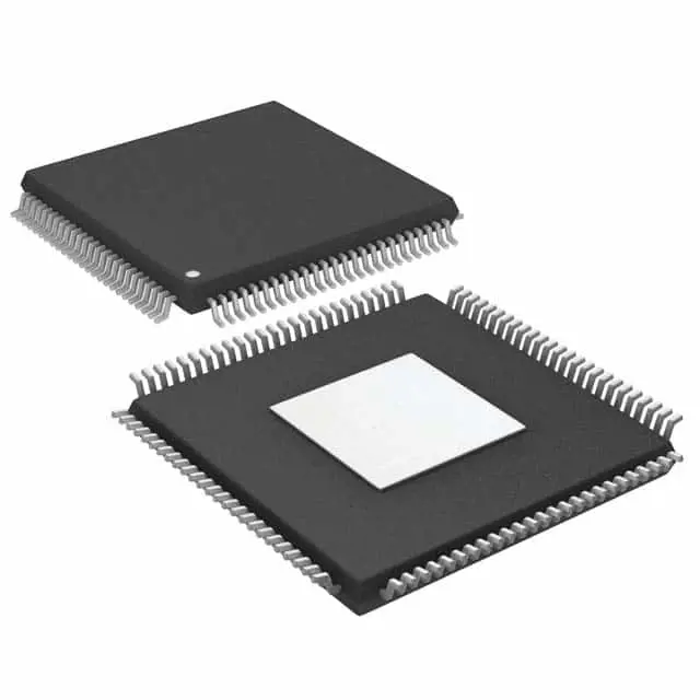
画像は参照用のみです。
5M80ZT100C5N
IC CPLD 64MC 7.5NS 100TQFP
- メーカー
- Mfr。パート #5M80ZT100C5N
- パッケージ TQFP-100
- データシート
- 在庫中4887
100% オリジナル &新しい
出荷の準備ができている24時間
365日の保証
RFQおよびもっと割引を得る
仕様
| Package | Tray |
| Series | MAX® V |
| ProductStatus | Active |
| ProgrammableType | In System Programmable |
| DelayTimetpd(1)Max | 7.5 ns |
| VoltageSupply-Internal | 1.71V ~ 1.89V |
| NumberofLogicElements/Blocks | 80 |
| NumberofMacrocells | 64 |
| NumberofI/O | 79 |
| OperatingTemperature | 0°C ~ 85°C (TJ) |
| MountingType | Surface Mount |
| Package/Case | 100-TQFP |
概要
Description
The 5M80ZT100C5N is a type of field-programmable gate array (FPGA) developed by Microsemi, part of the Microchip Technology family. It belongs to the SmartFusion and IGLOO series, which are known for their low power consumption and embedded features, such as ARM Cortex-M3 processors and analog components.
The 5M80ZT100C5N is tailored for applications requiring high performance and flexibility, making it suitable for embedded systems, industrial automation, aerospace, and defense applications. It offers a range of configurable logic blocks, digital signal processing capabilities, and memory resources, allowing designers to implement custom functions and algorithms.
Key attributes include support for various I/O standards, built-in security features, and power management options. Its architecture enables rapid prototyping and efficient design iterations, making it a popular choice for developers looking to create specialized hardware solutions without the high costs of custom ASIC designs. Overall, the 5M80ZT100C5N provides a versatile platform for a wide array of digital and embedded applications.
The 5M80ZT100C5N is tailored for applications requiring high performance and flexibility, making it suitable for embedded systems, industrial automation, aerospace, and defense applications. It offers a range of configurable logic blocks, digital signal processing capabilities, and memory resources, allowing designers to implement custom functions and algorithms.
Key attributes include support for various I/O standards, built-in security features, and power management options. Its architecture enables rapid prototyping and efficient design iterations, making it a popular choice for developers looking to create specialized hardware solutions without the high costs of custom ASIC designs. Overall, the 5M80ZT100C5N provides a versatile platform for a wide array of digital and embedded applications.
Features
The 5M80ZT100C5N is a member of the Intel MAX 10 FPGA family, featuring a low-power, single-chip architecture suitable for various applications. Key features include:
1. Logic Elements: Up to 80,000 logic elements, allowing for complex designs.
2. Memory: Integrated embedded memory blocks for efficient data storage and access.
3. I/O Pins: A versatile set of I/O pins supporting various voltage levels and standards.
4. Low Power Consumption: Optimized for energy efficiency, making it suitable for battery-powered devices.
5. Embedded DSP Blocks: Includes dedicated digital signal processing blocks for high-performance signal processing tasks.
6. Flexible Configuration: Programmable architecture for custom applications, including real-time processing and control systems.
7. Integrated ADC: Some configurations may offer integrated analog-to-digital converters for mixed-signal applications.
8. Development Support: Compatible with Intel’s Quartus Prime design software for streamlined development and design implementation.
These features make the 5M80ZT100C5N ideal for applications in IoT, automotive, and industrial control systems.
1. Logic Elements: Up to 80,000 logic elements, allowing for complex designs.
2. Memory: Integrated embedded memory blocks for efficient data storage and access.
3. I/O Pins: A versatile set of I/O pins supporting various voltage levels and standards.
4. Low Power Consumption: Optimized for energy efficiency, making it suitable for battery-powered devices.
5. Embedded DSP Blocks: Includes dedicated digital signal processing blocks for high-performance signal processing tasks.
6. Flexible Configuration: Programmable architecture for custom applications, including real-time processing and control systems.
7. Integrated ADC: Some configurations may offer integrated analog-to-digital converters for mixed-signal applications.
8. Development Support: Compatible with Intel’s Quartus Prime design software for streamlined development and design implementation.
These features make the 5M80ZT100C5N ideal for applications in IoT, automotive, and industrial control systems.
Package
The 5M80ZT100C5N is packaged in a FGGA (Fine Pitch Ball Grid Array) form factor. This packaging type is designed for high-density applications, allowing for a compact layout and efficient thermal performance.
Pinout
The 5M80ZT100C5N is a member of the Intel/Altera MAX 10 FPGA family. It features a pin count of 100 pins.
The device is designed for various applications and offers a range of functionalities, including:
1. Logic and I/O: Supports configurable logic blocks and I/O pins that can be programmed for various signal standards.
2. Memory: Includes built-in memory features, such as RAM and ROM, for storing data.
3. Programmable Interconnect: Allows flexible connections between different blocks within the FPGA.
4. Embedded Features: Supports features like phase-locked loops (PLLs) and digital signal processing (DSP) blocks, depending on the specific configuration.
5. Versatile Applications: Suitable for applications in industrial control, automotive, and consumer electronics.
The 5M80ZT100C5N is well-suited for low-power, cost-effective solutions in embedded systems.
The device is designed for various applications and offers a range of functionalities, including:
1. Logic and I/O: Supports configurable logic blocks and I/O pins that can be programmed for various signal standards.
2. Memory: Includes built-in memory features, such as RAM and ROM, for storing data.
3. Programmable Interconnect: Allows flexible connections between different blocks within the FPGA.
4. Embedded Features: Supports features like phase-locked loops (PLLs) and digital signal processing (DSP) blocks, depending on the specific configuration.
5. Versatile Applications: Suitable for applications in industrial control, automotive, and consumer electronics.
The 5M80ZT100C5N is well-suited for low-power, cost-effective solutions in embedded systems.
Manufacturer
The manufacturer of the 5M80ZT100C5N is Microchip Technology Inc. Microchip is a leading provider of microcontroller and analog semiconductors, specializing in microcontrollers, memory, and related technologies. Founded in 1989, the company is headquartered in Chandler, Arizona. Microchip serves a diverse range of industries, including automotive, industrial, consumer, and communications, providing solutions for embedded systems, IoT applications, and more. The 5M80ZT100C5N is part of their FPGA (Field-Programmable Gate Array) product line, indicating their focus on programmable logic devices that allow for flexible hardware design.
Application
The 5M80ZT100C5N is a high-performance FPGA (Field-Programmable Gate Array) primarily used in applications such as digital signal processing, telecommunications, data acquisition systems, industrial automation, and embedded systems. Its flexibility allows for rapid prototyping and implementation of custom hardware solutions in sectors like automotive, aerospace, and medical devices.
Equivalent
The 5M80ZT100C5N is a part of the Intel/Altera MAX 10 FPGA family. Equivalent products include the Lattice MachXO2 series, Xilinx Spartan-6, and Intel Cyclone IV FPGAs. When looking for alternatives, consider factors like logic density, I/O capabilities, and specific application requirements. Always verify specific features and specifications to ensure compatibility.
出荷
出荷方法私たち
DHL、FedEx、TNT、UPS、またはあなたの選択の他の運送業者を通じてグローバルな出荷サービスを提供します。
出荷料参照(DHL/FedEx):
DHL の: 配送費は25ドル〜45ドル(0.5kg)の範囲で、推定配送時間は2〜5営業日です。
フェデックス: 配送費は25ドル〜40ドル(0.5kg)の範囲で、推定配送時間は3〜7営業日。
UPS の: 配送費は25ドル〜45ドル(0.5kg)の範囲で、推定配送時間は3〜7営業日。
TNT社: 配送費は25ドル〜65ドル(0.5kg)の範囲で、推定配送時間は3〜7営業日。
EMS: 配送料金は30〜50ドル(0.5kg)の範囲で、推定配送時間は7〜15営業日です。
登録航空郵便: 配送費は2〜4ドル(0.1kg)で、推定配送時間は5〜20営業日です。
支払い
Payment Methods
支払い期間は100%前払いです。
現在、下記の支払い方法のみを受け入れています。:
1. ペイパル
2. クレジット・デビットカード
3. ワイヤー 転送
類似
-
![MX25V1635FZNI]() MX25V1635FZNI
MX25V1635FZNI
Macronix
-
![MX66U1G45GXDI00]() MX66U1G45GXDI00
MX66U1G45GXDI00
Macronix
-
![MX25V16066M1I02]() MX25V16066M1I02
MX25V16066M1I02
Macronix
-
![MX25V16066M2I02]() MX25V16066M2I02
MX25V16066M2I02
Macronix
-
![MX25L25673GMI-10G]() MX25L25673GMI-10G
MX25L25673GMI-10G
Macronix
-
![MX25U51279GXDR00]() MX25U51279GXDR00
MX25U51279GXDR00
Macronix
-
![MX25U25643GZNI00]() MX25U25643GZNI00
MX25U25643GZNI00
Macronix
-
![MX25U3232FZBI02]() MX25U3232FZBI02
MX25U3232FZBI02
Macronix
-
![MX25L6433FM2I-08G]() MX25L6433FM2I-08G
MX25L6433FM2I-08G
Macronix
-
![MX25U6435FM2I-10G]() MX25U6435FM2I-10G
MX25U6435FM2I-10G
Macronix
-
![MX25L12833FM2I-10G]() MX25L12833FM2I-10..
MX25L12833FM2I-10..
Macronix
-
![MX25L12833FZ2I-10G]() MX25L12833FZ2I-10..
MX25L12833FZ2I-10..
Macronix





