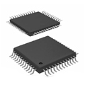
画像は参照用のみです。
5M80ZM68C4N
IC CPLD 64MC 7.5NS 68MBGA
- メーカー
- Mfr。パート #5M80ZM68C4N
- パッケージ BGA-68
- データシート
- 在庫中5647
100% オリジナル &新しい
出荷の準備ができている24時間
365日の保証
RFQおよびもっと割引を得る
仕様
| Package | Tray |
| Series | MAX® V |
| ProductStatus | Active |
| ProgrammableType | In System Programmable |
| DelayTimetpd(1)Max | 7.5 ns |
| VoltageSupply-Internal | 1.71V ~ 1.89V |
| NumberofLogicElements/Blocks | 80 |
| NumberofMacrocells | 64 |
| NumberofI/O | 52 |
| OperatingTemperature | 0°C ~ 85°C (TJ) |
| MountingType | Surface Mount |
| Package/Case | 68-TFBGA |
概要
Description
The code "5M80ZM68C4N" appears to be a specific identifier, possibly related to a product, component, or model number. However, without additional context, it's challenging to determine its exact significance. It may belong to various industries, including electronics, automotive, or consumer goods. Each segment of the code could represent different attributes such as series, version, specifications, or manufacturing details.
If you have a specific industry or application in mind related to this code, please provide more details for a more tailored introduction.
If you have a specific industry or application in mind related to this code, please provide more details for a more tailored introduction.
Features
The 5M80ZM68C4N is a field-programmable gate array (FPGA) from Intel's MAX 10 series. Key features include:
1. Density: Offers up to 50,000 logic elements, enabling complex designs.
2. Embedded Memory: Supports up to 2.5 Mbits of embedded memory, facilitating data storage and processing.
3. I/O Flexibility: Features up to 68 I/O pins with various signaling standards, supporting a wide range of applications.
4. Analog Integration: Includes embedded analog-to-digital converters (ADCs) for analog signal processing.
5. Low Power: Designed for low power consumption, making it suitable for battery-operated devices.
6. Single-Chip Solution: Combines logic, memory, and I/O functions, reducing PCB space and design complexity.
7. Development Tools: Compatible with Intel's Quartus Prime software for easy design, simulation, and debugging.
These features make the 5M80ZM68C4N ideal for applications in industrial control, automotive systems, and consumer electronics.
1. Density: Offers up to 50,000 logic elements, enabling complex designs.
2. Embedded Memory: Supports up to 2.5 Mbits of embedded memory, facilitating data storage and processing.
3. I/O Flexibility: Features up to 68 I/O pins with various signaling standards, supporting a wide range of applications.
4. Analog Integration: Includes embedded analog-to-digital converters (ADCs) for analog signal processing.
5. Low Power: Designed for low power consumption, making it suitable for battery-operated devices.
6. Single-Chip Solution: Combines logic, memory, and I/O functions, reducing PCB space and design complexity.
7. Development Tools: Compatible with Intel's Quartus Prime software for easy design, simulation, and debugging.
These features make the 5M80ZM68C4N ideal for applications in industrial control, automotive systems, and consumer electronics.
Package
The 5M80ZM68C4N is a FPGA (Field-Programmable Gate Array) from Intel's MAX 10 family. It comes in a 68-pin TQFP (Thin Quad Flat Package) package type. This package type allows for efficient mounting on PCBs and is suitable for various applications in digital design and prototyping.
Pinout
The 5M80ZM68C4N is a member of the Intel MAX 10 FPGA family. It features a total of 68 pins. The primary functions of these pins include:
1. I/O Pins: Configurable for general-purpose input/output operations.
2. Dedicated Configuration Pins: Used to load configuration data into the FPGA.
3. Power Supply Pins: Provide power to the FPGA.
4. Clock Pins: For inputting clock signals for synchronous operations.
5. JTAG Pins: For programming and debugging the FPGA via the Joint Test Action Group interface.
The FPGA supports a range of digital logic functions and is used in various applications such as communications, automotive, and industrial systems.
1. I/O Pins: Configurable for general-purpose input/output operations.
2. Dedicated Configuration Pins: Used to load configuration data into the FPGA.
3. Power Supply Pins: Provide power to the FPGA.
4. Clock Pins: For inputting clock signals for synchronous operations.
5. JTAG Pins: For programming and debugging the FPGA via the Joint Test Action Group interface.
The FPGA supports a range of digital logic functions and is used in various applications such as communications, automotive, and industrial systems.
Manufacturer
The 5M80ZM68C4N is manufactured by Intel Corporation. Intel is a multinational technology company known primarily for its semiconductor products, including microprocessors, chipsets, and integrated circuits. Founded in 1968, it is one of the world's largest and most influential firms in the tech industry. Intel plays a pivotal role in the development of computing technology, producing components that power a wide range of devices, from personal computers to data centers and embedded systems. The company's innovations have significantly impacted the evolution of computing and technology globally.
Application
The 5M80ZM68C4N is an FPGA (Field Programmable Gate Array) primarily used in various applications such as digital signal processing, embedded system design, telecommunications, automotive systems, and industrial automation. It supports high-performance computation and can be utilized in custom hardware designs, prototyping, and real-time data processing tasks across diverse fields, including robotics and consumer electronics.
Equivalent
The 5M80ZM68C4N chip is a member of the Intel/Altera MAX 10 FPGA family. Equivalent products include the 5M80Z, 5M40Z, and 5M160Z series, depending on specific requirements like I/O count, speed grade, and memory size. For specific applications, look at other FPGA families like Xilinx Spartan or Lattice iCE40, but ensure they meet your design criteria. Always refer to datasheets for compatibility.
出荷
出荷方法私たち
DHL、FedEx、TNT、UPS、またはあなたの選択の他の運送業者を通じてグローバルな出荷サービスを提供します。
出荷料参照(DHL/FedEx):
DHL の: 配送費は25ドル〜45ドル(0.5kg)の範囲で、推定配送時間は2〜5営業日です。
フェデックス: 配送費は25ドル〜40ドル(0.5kg)の範囲で、推定配送時間は3〜7営業日。
UPS の: 配送費は25ドル〜45ドル(0.5kg)の範囲で、推定配送時間は3〜7営業日。
TNT社: 配送費は25ドル〜65ドル(0.5kg)の範囲で、推定配送時間は3〜7営業日。
EMS: 配送料金は30〜50ドル(0.5kg)の範囲で、推定配送時間は7〜15営業日です。
登録航空郵便: 配送費は2〜4ドル(0.1kg)で、推定配送時間は5〜20営業日です。
支払い
Payment Methods
支払い期間は100%前払いです。
現在、下記の支払い方法のみを受け入れています。:
1. ペイパル
2. クレジット・デビットカード
3. ワイヤー 転送
類似
-
![MX25R8035FM1IL0]() MX25R8035FM1IL0
Macronix
-
![MX25L3233FZBI-08Q]() MX25L3233FZBI-08Q
Macronix
-
![MX25V1635FZNQ03]() MX25V1635FZNQ03
Macronix
-
![MX25V16066M2I02]() MX25V16066M2I02
Macronix
-
![MX25L25673GMI-08G]() MX25L25673GMI-08G
Macronix
-
![MX25L25673GMI-10G]() MX25L25673GMI-10G
Macronix
-
![MX25U51279GXDR00]() MX25U51279GXDR00
Macronix
-
![MX25U25643GZNI00]() MX25U25643GZNI00
Macronix
-
![MX25L12833FZ2I-10G]() MX25L12833FZ2I-10..
Macronix
-
![MX25L12833FZNI-10G]() MX25L12833FZNI-10..
Macronix
-
![MX25U25645GXDI00]() MX25U25645GXDI00
Macronix
-
![MX25L12835FZ2I-10G]() MX25L12835FZ2I-10..
Macronix