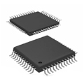
画像は参照用のみです。
10M40DCF256A7G
IC FPGA 178 I/O 256FBGA
- メーカー
- Mfr。パート #10M40DCF256A7G
- パッケージ 256-LBGA
- データシート
- 在庫中3281
100% オリジナル &新しい
出荷の準備ができている24時間
365日の保証
RFQおよびもっと割引を得る
仕様
| Package | Tray |
| Series | MAX® 10 |
| ProductStatus | Active |
| NumberofLABs/CLBs | 2500 |
| NumberofLogicElements/Cells | 40000 |
| TotalRAMBits | 1290240 |
| NumberofI/O | 178 |
| Voltage-Supply | 1.15V ~ 1.25V |
| MountingType | Surface Mount |
| OperatingTemperature | -40°C ~ 125°C (TJ) |
| Package/Case | 256-LBGA |
概要
Description
The 10M40DCF256A7G is a part of Intel's MAX 10 FPGA family, designed for low-power, cost-sensitive applications. It features 40,000 logic elements and includes a range of integrated resources such as DSP blocks, memory, and I/O pins. The device operates at 3.3V and is built using a flash-based architecture, which allows for in-system reconfiguration and faster boot times compared to traditional SRAM-based FPGAs.
The "DCF256" designation indicates this FPGA has 256 pins, facilitating connections to various peripherals and other components. The "A7G" suffix refers to specific package types and temperature ranges, optimizing it for diverse environments and applications.
This FPGA is particularly suitable for applications like industrial automation, communications, and automotive systems, where flexibility, efficiency, and reliability are crucial. The MAX 10 series also supports various development tools, making it easier for engineers to implement complex designs efficiently.
The "DCF256" designation indicates this FPGA has 256 pins, facilitating connections to various peripherals and other components. The "A7G" suffix refers to specific package types and temperature ranges, optimizing it for diverse environments and applications.
This FPGA is particularly suitable for applications like industrial automation, communications, and automotive systems, where flexibility, efficiency, and reliability are crucial. The MAX 10 series also supports various development tools, making it easier for engineers to implement complex designs efficiently.
Features
The 10M40DCF256A7G is a part of Intel's MAX 10 FPGA family, specifically designed for low-power, cost-effective applications. Key features include:
1. Density: 40,000 logic elements (LEs) providing ample resources for various designs.
2. I/O Pins: Up to 256 user I/O pins, allowing extensive interfacing capabilities.
3. Flash Memory: Integrated non-volatile flash memory for configuration storage.
4. Power Efficiency: Low static and dynamic power consumption, suitable for battery-operated devices.
5. Programmable Logic: Supports a range of digital logic functions, including combinational and sequential logic.
6. DSP Blocks: Includes dedicated DSP blocks for high-performance arithmetic and signal processing tasks.
7. Flexible Interface: Supports various I/O standards, including LVCMOS, LVTTL, and others.
8. Development Tools: Compatible with Intel Quartus Prime software for design implementation.
9. Embedded Features: Options for embedded memory blocks and phase-locked loops (PLLs) for timing adjustments.
This FPGA is ideal for applications in automotive, industrial, and consumer electronics, where flexibility and efficiency are paramount.
1. Density: 40,000 logic elements (LEs) providing ample resources for various designs.
2. I/O Pins: Up to 256 user I/O pins, allowing extensive interfacing capabilities.
3. Flash Memory: Integrated non-volatile flash memory for configuration storage.
4. Power Efficiency: Low static and dynamic power consumption, suitable for battery-operated devices.
5. Programmable Logic: Supports a range of digital logic functions, including combinational and sequential logic.
6. DSP Blocks: Includes dedicated DSP blocks for high-performance arithmetic and signal processing tasks.
7. Flexible Interface: Supports various I/O standards, including LVCMOS, LVTTL, and others.
8. Development Tools: Compatible with Intel Quartus Prime software for design implementation.
9. Embedded Features: Options for embedded memory blocks and phase-locked loops (PLLs) for timing adjustments.
This FPGA is ideal for applications in automotive, industrial, and consumer electronics, where flexibility and efficiency are paramount.
Package
The 10M40DCF256A7G is packaged in a Fine Line BGA (Ball Grid Array) form factor. It features a 256-ball configuration, allowing for efficient heat dissipation and compact design suitable for various applications in FPGA systems.
Pinout
The 10M40DCF256A7G is a FPGA (Field-Programmable Gate Array) from Intel's MAX 10 family. It features a pin count of 256 pins.
In terms of functionality, the 10M40DCF256A7G is designed for various applications, including digital signal processing, control systems, and custom logic implementations. It offers capabilities like configurable I/O, embedded memory, and high-speed performance with a maximum operating frequency of 200 MHz, making it suitable for both consumer and industrial applications.
Additionally, the device includes integrated analog features and supports various communication protocols, enhancing its versatility for different design needs.
In terms of functionality, the 10M40DCF256A7G is designed for various applications, including digital signal processing, control systems, and custom logic implementations. It offers capabilities like configurable I/O, embedded memory, and high-speed performance with a maximum operating frequency of 200 MHz, making it suitable for both consumer and industrial applications.
Additionally, the device includes integrated analog features and supports various communication protocols, enhancing its versatility for different design needs.
Manufacturer
The manufacturer of the 10M40DCF256A7G is Intel Corporation. Intel is a multinational technology company primarily known for designing and manufacturing semiconductor products, particularly microprocessors and integrated circuits. Founded in 1968, Intel has been a leader in the computer hardware industry, playing a crucial role in the development of modern computing technologies. Its products are widely used in personal computers, servers, and embedded systems. The 10M40DCF256A7G is a member of Intel’s Max 10 FPGA family, which is designed for a variety of applications, including industrial, automotive, and consumer electronic systems.
Application
The 10M40DCF256A7G is a low-power, FPGA (Field Programmable Gate Array) device used in application areas such as digital signal processing, telecommunications, embedded systems, industrial control, and automotive systems. Its versatility allows for custom hardware implementations in signal conditioning, data acquisition, image processing, and machine learning applications, supporting a wide range of embedded applications.
Equivalent
The 10M40DCF256A7G chip is an FPGA from Intel's MAX 10 series. Equivalent products include the Lattice Semiconductor ICE40 series, such as the ICE40LP or ICE40HX FPGAs, and the Xilinx Artix-7 series, such as the XC7A35T. Specific alternatives may vary based on performance, I/O requirements, and power consumption, so it’s essential to evaluate based on your project needs.
出荷
出荷方法私たち
DHL、FedEx、TNT、UPS、またはあなたの選択の他の運送業者を通じてグローバルな出荷サービスを提供します。
出荷料参照(DHL/FedEx):
DHL の: 配送費は25ドル〜45ドル(0.5kg)の範囲で、推定配送時間は2〜5営業日です。
フェデックス: 配送費は25ドル〜40ドル(0.5kg)の範囲で、推定配送時間は3〜7営業日。
UPS の: 配送費は25ドル〜45ドル(0.5kg)の範囲で、推定配送時間は3〜7営業日。
TNT社: 配送費は25ドル〜65ドル(0.5kg)の範囲で、推定配送時間は3〜7営業日。
EMS: 配送料金は30〜50ドル(0.5kg)の範囲で、推定配送時間は7〜15営業日です。
登録航空郵便: 配送費は2〜4ドル(0.1kg)で、推定配送時間は5〜20営業日です。
支払い
Payment Methods
支払い期間は100%前払いです。
現在、下記の支払い方法のみを受け入れています。:
1. ペイパル
2. クレジット・デビットカード
3. ワイヤー 転送
類似
-
![MX25R8035FM1IL0]() MX25R8035FM1IL0
Macronix
-
![MX25L3233FZBI-08Q]() MX25L3233FZBI-08Q
Macronix
-
![MX25V1635FZNI]() MX25V1635FZNI
Macronix
-
![MX66U1G45GXDI00]() MX66U1G45GXDI00
Macronix
-
![MX25V2033FM1I]() MX25V2033FM1I
Macronix
-
![MX30LF2G28AD-TI]() MX30LF2G28AD-TI
Macronix
-
![MX25L8035EM2I-10G]() MX25L8035EM2I-10G
Macronix
-
![MX25L25673GMI-08G]() MX25L25673GMI-08G
Macronix
-
![MX25U25643GZNI00]() MX25U25643GZNI00
Macronix
-
![MX25L2006EM1I-12G]() MX25L2006EM1I-12G
Macronix
-
![MX25V1635FM2I]() MX25V1635FM2I
Macronix
-
![MX25U3232FZBI02]() MX25U3232FZBI02
Macronix